

Organic EL element having cathode buffer layer
An organic and cathode technology, applied in the direction of organic semiconductor devices, electrical components, electrical solid devices, etc., can solve the problems of inability to exert electron injection and transport performance, increase of driving voltage, and obstruction of electron transport to the light-emitting layer, so as to prevent the driving voltage. Effects of increasing and decreasing driving voltage and suppressing current leakage
- Summary
- Abstract
- Description
- Claims
- Application Information
AI Technical Summary
Problems solved by technology
Method used
Image

Examples
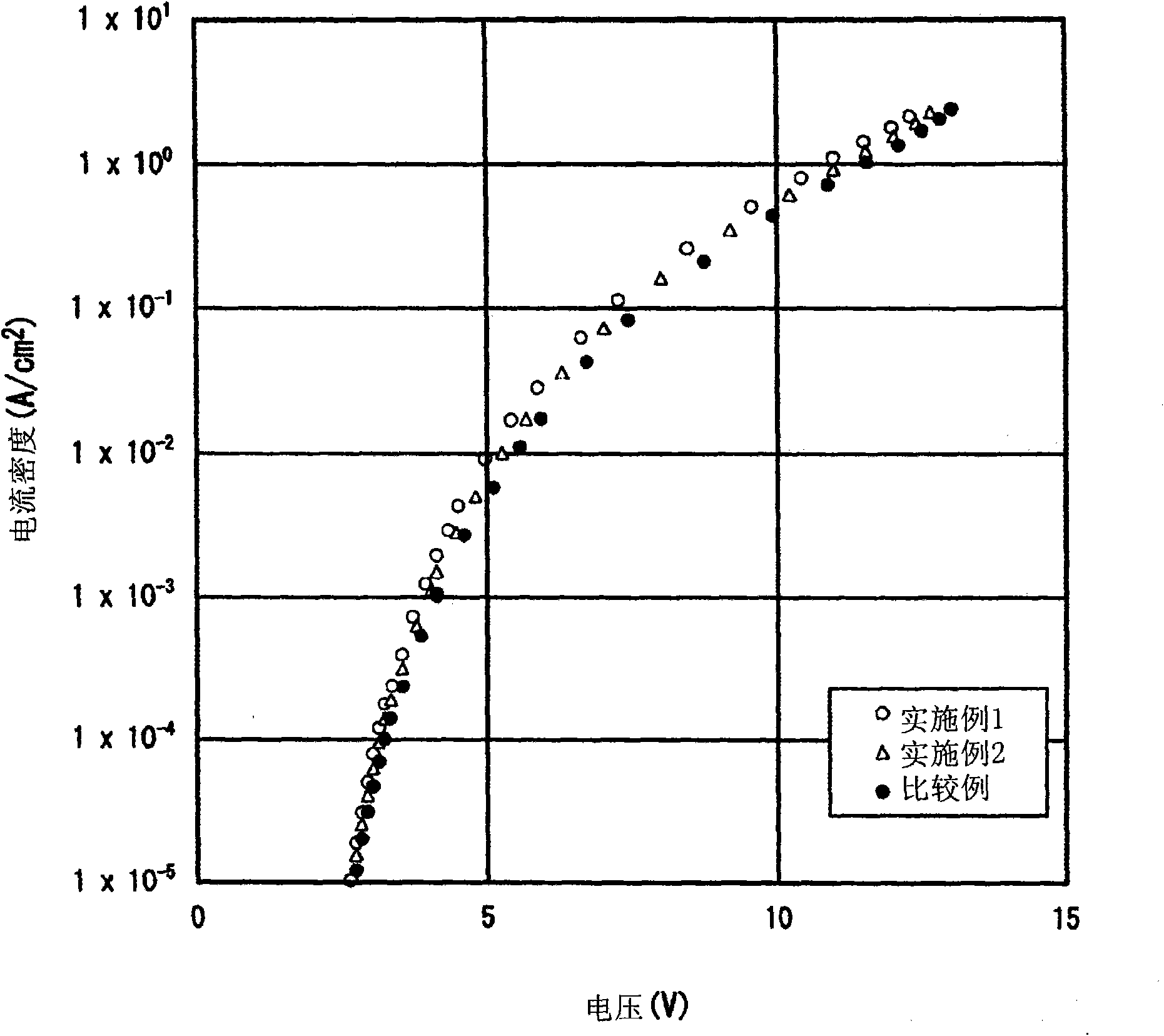
Embodiment 1
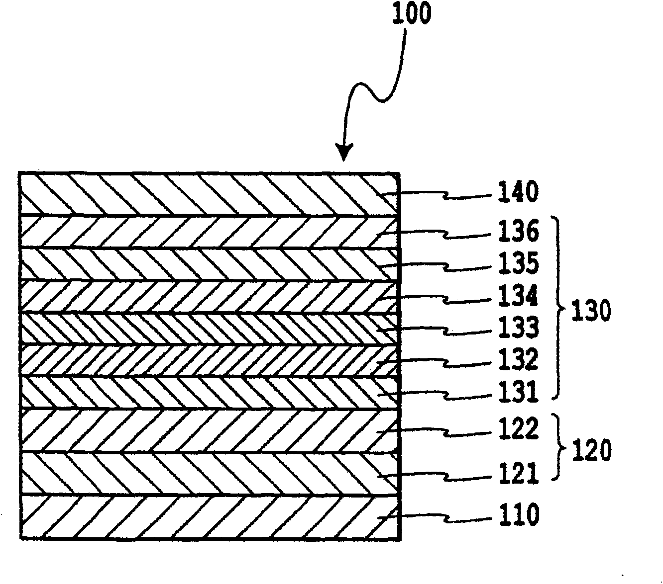
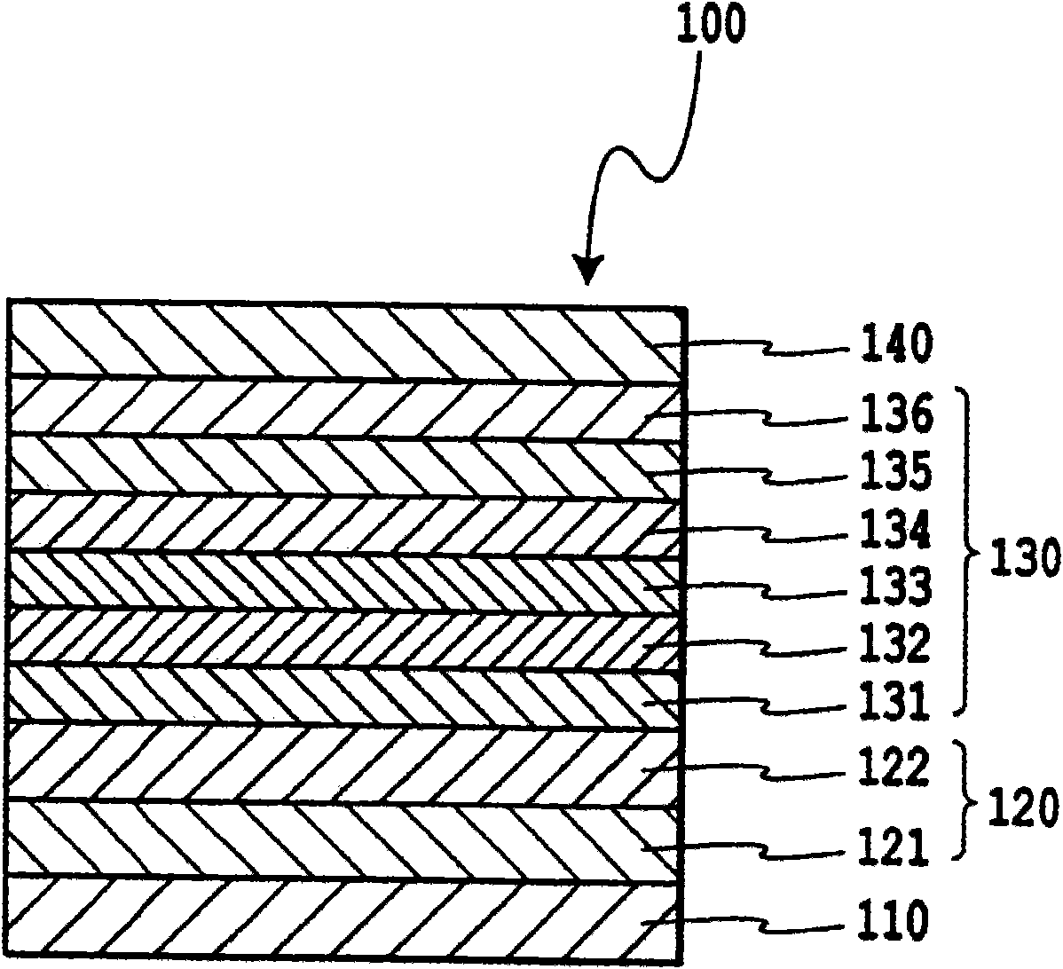
[0083] In this embodiment, a cathode 120 formed of Ag and IZO, a cathode buffer layer 131, an electron injection and transport layer 132, a light-emitting layer 133, a hole transport layer 134, a hole injection and transport layer 135, and an anode buffer layer are sequentially formed on the substrate 110. Examples of organic EL elements of layer 136 and anode 140 .
[0084] On a glass substrate 110 (vertical 50 mm x lateral 50 mm x thickness 0.7 mm, 1737 glass produced by Corning), an Ag film with a thickness of 100 nm was formed using a DC magnetron sputtering method. Then, on the upper surface of the Ag film, a DC magnetron sputtering method (target: In 2 O 3 +10wt%ZnO, discharge gas: Ar+0.5%O 2 , discharge pressure: 0.3Pa, discharge power: 1.45W / cm 3 , the substrate conveying speed is 162 mm / min), and an IZO film with a film thickness of 110 nm is formed. Next, the laminated body of the Ag film and the IZO film was processed into a strip shape with a width of 2 mm by p...
Embodiment 2
[0089] The procedure of 1 was repeated except that the film thickness of the cathode buffer layer 131 was changed to 50 nm, and an organic EL element was produced.
PUM
 Abstract
Description
Claims
Application Information