Silicon chip phosphorous diffusion impurity removal process for manufacturing solar cell

A solar cell and phosphorus diffusion technology, applied in the direction of diffusion/doping, crystal growth, after treatment, etc., can solve the problem of not being able to effectively reduce metal impurities, and achieve the effect of improving light conversion efficiency and reducing content

Inactive Publication Date: 2012-06-27
ZHEJIANG UNIV
View PDF0 Cites 0 Cited by
  • Summary
  • Abstract
  • Description
  • Claims
  • Application Information

AI Technical Summary

Problems solved by technology

[0008] The present invention provides a silicon wafer phosphorus diffusion gettering process for manufacturing solar cells, which solves the problem that the existing process cannot effectively reduce metal impurities in low-quality silicon materials

Method used


Image

  • Silicon chip phosphorous diffusion impurity removal process for manufacturing solar cell
  • Silicon chip phosphorous diffusion impurity removal process for manufacturing solar cell
  • Silicon chip phosphorous diffusion impurity removal process for manufacturing solar cell

Examples


Embodiment 1

[0028] (1) Take the original cast polysilicon wafer, such as figure 2 As shown in (a), the minority carrier lifetime is about 4 μs after testing;

[0029] (2) Spin-coat both sides of the above-mentioned silicon wafer with a phosphorus source (p-854, Honeywell), and then pre-bake at 200°C for 10 minutes to remove organic matter;

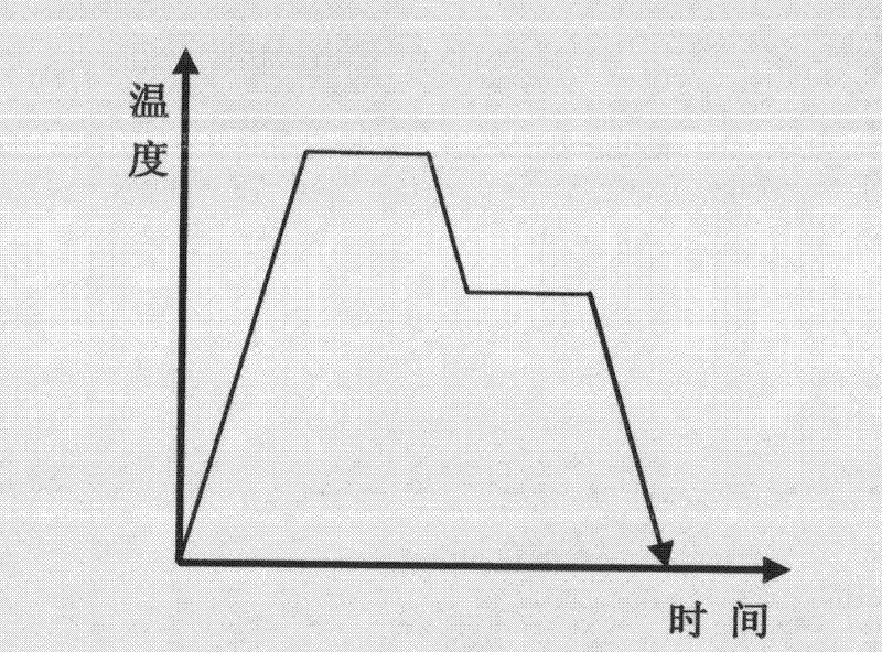
[0030] (3) Pass the protective gas (argon) into the diffusion furnace. The diffusion furnace does not need to be closed, and the air pressure is about 1 atmosphere. Place the baked silicon wafer in the diffusion furnace, and control the temperature in the furnace to 1000°C , keep warm for 30min; then control the temperature in the furnace to 700°C, keep warm for 60min, and take the same treated silicon wafer and place it in a diffusion furnace with a furnace temperature of 900°C for 60min, as a control group;

[0031] (4) Take out the silicon chip, after cooling, remove the phosphosilicate glass layer with dilute HF (volume concentration 10%);

[0...

Embodiment 2

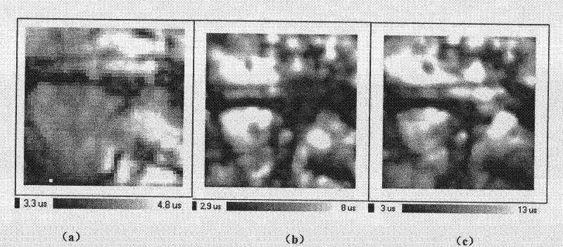
[0034] (1) Take the original single crystal silicon wafer, the minority carrier lifetime is about 6μs after detection, after iron contamination, the minority carrier lifetime drops to 0.4μs, as image 3 as shown in (a);

[0035] (2) Spin-coat both sides of the above-mentioned monocrystalline silicon wafer with a phosphorus source (p-854, Honeywell), and then pre-bake at 200°C for 10 minutes to remove organic matter;

[0036] (3) Pass the protective gas (argon gas) into the diffusion furnace. The diffusion furnace does not need to be closed. 850°C, keep warm for 30 minutes, then control the temperature in the furnace to 700°C, keep warm for 90 minutes, and take the same treated monocrystalline silicon wafers and place them in a diffusion furnace with a furnace temperature of 900°C for 120 minutes, as a control group;

[0037] (4) Take out the silicon chip, after cooling, remove the phosphosilicate glass layer with dilute HF (volume concentration 10%);

[0038] Such as image...

Embodiment 3

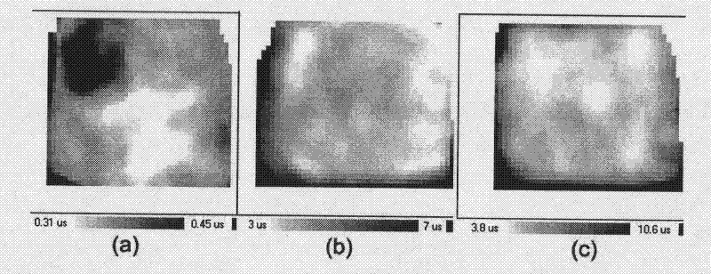
[0040] (1) Take native polysilicon wafers, such as Figure 4 As shown in (a), the minority carrier lifetime is about 3.5 μs after detection. After iron contamination, as Figure 4 As shown in (b), the minority carrier lifetime drops to 0.3μs;

[0041] (2) Spin-coat both sides of the above-mentioned polysilicon wafer with a phosphorus source (p-854, Honeywell), and then pre-bake at 200° C. for 10 minutes;

[0042] (3) Pass the protective gas (argon gas) into the diffusion furnace. The diffusion furnace does not need to be closed. 900°C, heat preservation for 10 minutes, then control the temperature in the furnace to 650°C, heat preservation for 50 minutes, and at the same time take the same treated monocrystalline silicon wafers and place them in a diffusion furnace with a furnace temperature of 900°C for 60 minutes, as a control group;

[0043] (4) Take out the silicon chip, after cooling, remove the phosphosilicate glass layer with dilute HF (volume concentration 10%);

[...


PUM


Abstract

The invention discloses a silicon chip phosphorous diffusion impurity removal process for manufacturing a solar cell, which comprises the following steps of: coating a phosphorous source on the surface of a silicon chip or carrying POCl3 into a diffusion furnace tube by carrier gas, placing the silicon chip at the temperature of between 800 and 1,050 DEG C and preserving the heat for 10 to 60 minutes under protective atmosphere, then placing the silicon chip at the temperature of between 500 and 800 DEG C and preserving the heat for 20 to 60 minutes, cooling the silicon chip and removing a phosphorous silicon glass layer. The process can effectively reduce the metal impurity content of silicon matrix and improve the optical transformation efficiency of the solar cell by adopting a variable temperature impurity absorption mode and combining the advantages that the impurity is easily dissolved and released at the high temperature and effectively captured by an impurity absorption layer at the low temperature.

Description

technical field [0001] The invention relates to the technical field of manufacturing silicon solar cells, in particular to a silicon wafer phosphorus diffusion gettering process for manufacturing solar cells. Background technique [0002] Since entering the 21st century, with the gradual depletion of primary energy and the increasing demand for energy, human beings are facing more and more serious energy crises. The development and utilization of renewable energy has become the hope to solve the human energy crisis. Among all renewable energy sources, solar energy is a widely distributed and inexhaustible clean energy source with great application prospects. Solar cells are semiconductor devices that convert solar energy into electricity without producing any pollution. Therefore, the development and utilization of solar cells has become a research hotspot worldwide. [0003] At present, crystalline silicon is the most important solar cell material, with a market share of...

Claims


Application Information

Patent Timeline
Patent Type & Authority Patents(China)
IPC IPC(8): C30B31/04
Inventor 杨德仁李晓强余学功
Owner ZHEJIANG UNIV
Why Eureka
Try Eureka