GaAs unijunction solar cell
A solar cell and single-junction technology, applied in circuits, electrical components, photovoltaic power generation, etc., can solve problems such as increased production costs, difficult production, complex and precise manufacturing processes, etc., and achieve the effect of broadening the absorption band and improving photoelectric conversion efficiency
- Summary
- Abstract
- Description
- Claims
- Application Information
AI Technical Summary
Problems solved by technology
Method used
Image

Examples
Embodiment 1
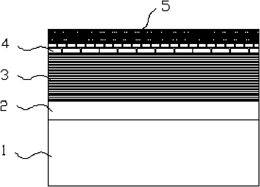
[0017] 1) On the GaAs substrate 1, a buffer layer 2, a GaAs p-n junction 3, a window layer 4 and an ohmic contact layer 5 are sequentially grown by MOCVD method (such as figure 2 Shown), composed of GaAs single-junction solar cell epitaxial layer.
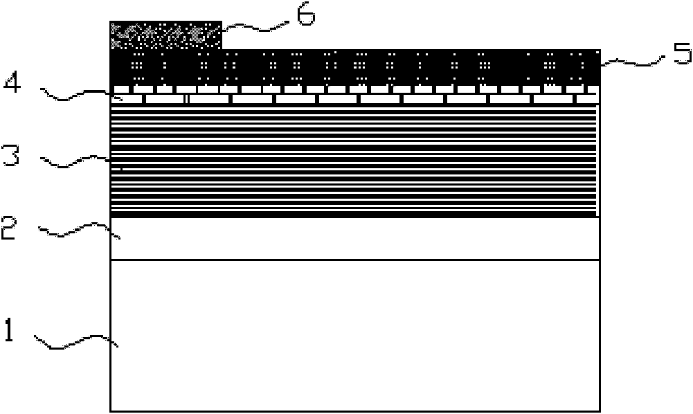
[0018] 2) The upper electrode 6 is prepared on the upper surface of the GaAs single-junction solar cell epitaxial layer by sequentially using the traditional processes of photolithography, electrode evaporation, alloying, and electrode thickening (such as image 3 shown).
[0019] 3) Etching away the ohmic contact layer 5 other than the bottom of the upper electrode 6 by a selective ICP etching method, so that a platform of the window layer 4 appears (such as Figure 4 shown).
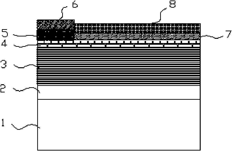
[0020] 4) On the platform of the window layer 4, deposit a layer of photoluminescent material CaS:Eu as the lower film 7 of the double-layer anti-reflection film. Deposit a layer of 80nm CaS film by magnetron sputtering, and then deposit a layer of 1nm ...
Embodiment 2
[0023] 1) On Ge substrate 1, buffer layer 2, GaAsp-n junction 3, window layer 4 and ohmic contact layer 5 are sequentially grown by MOCVD method (such as figure 2 Shown), composed of GaAs single-junction solar cell epitaxial layer.
[0024] 2) The upper electrode 6 is prepared on the upper surface of the epitaxial layer of the GaAs single-junction solar cell by sequentially using the traditional processes of photolithography, electrode evaporation, alloying, and electrode thickening (such as image 3 shown).
[0025] 3) Etch the ohmic contact layer 5 other than the bottom of the upper electrode 6 by selective wet etching, so that a platform of the window layer 4 appears (such as Figure 4 shown).
[0026] 4) On the platform of the window layer 4, deposit a layer of Sm-doped photoluminescent material CaS:Sm as the lower film 7 of the double-layer anti-reflection film. A layer of 80nm CaS film was deposited by atomic layer deposition, and a layer of 0.5nm SmF was deposited b...
Embodiment 3
[0028] 1) On the Ge substrate 1, the buffer layer 2, the GaAs p-n junction 3, the window layer 4 and the ohmic contact layer 5 are sequentially grown by the method of MBE (such as figure 2 Shown), composed of GaAs single-junction solar cell epitaxial layer.
[0029] 2) The upper electrode 6 is prepared on the upper surface of the epitaxial layer of the GaAs single-junction solar cell by sequentially using the traditional processes of photolithography, electrode evaporation, alloying, and electrode thickening (such as image 3 shown).
[0030] 3) Etch the ohmic contact layer 5 other than the bottom of the upper electrode 6 by selective wet etching, so that a platform of the window layer 4 appears (such as Figure 4 shown).
[0031] 4) On the platform of the window layer 4, deposit a layer of photoluminescent material CaS:Sm as the lower layer 7 of the double-layer anti-reflection film. Deposit a layer of 46nm CaS film by vacuum thermal evaporation, and then deposit a layer ...
PUM
 Abstract
Description
Claims
Application Information
 - R&D
- Intellectual Property
- Life Sciences
- Materials
- Tech Scout
- Unparalleled Data Quality
- Higher Quality Content
- 60% Fewer Hallucinations
Browse by: Latest US Patents, China's latest patents, Technical Efficacy Thesaurus, Application Domain, Technology Topic, Popular Technical Reports.
© 2025 PatSnap. All rights reserved.Legal|Privacy policy|Modern Slavery Act Transparency Statement|Sitemap|About US| Contact US: help@patsnap.com