Visible light-near infrared band solid state photocatalytic purifying film apparatus

A technology of catalytic purification and thin-film devices, applied in the field of photocatalysis, can solve problems such as air secondary pollution, impact on health, practicality and use range limitations, and achieve the effect of enhancing metal absorption

Pending Publication Date: 2017-08-15
SUZHOU YOUHAN INFORMATION TECH CO LTD
View PDF5 Cites 2 Cited by
  • Summary
  • Abstract
  • Description
  • Claims
  • Application Information

AI Technical Summary

Problems solved by technology

Since the ultraviolet part of sunlight is very weak, the photocatalytic ability of this type of product is greatly limited, especially in environments where ultraviolet rays are blocked, such as indoors, the photocatalytic reaction can hardly occur, and the practicability and scope of use are limited.
Additional costs if UV lamps are used
In addition, the catalysts used in photocatalytic purification products are generally nano-scale particles, which are dispersed in aqueous solution or attached to textiles and other carriers. If some nanoparticles are hidden in an environment without ultraviolet light during use and maintenance, it is bound to cause product damage. The waste and performance decline, and the shedding nanoparticles are easy to cause secondary pollution to the air, which will inevitably affect the health of the body if inhaled by the human body

Method used


Image

  • Visible light-near infrared band solid state photocatalytic purifying film apparatus
  • Visible light-near infrared band solid state photocatalytic purifying film apparatus
  • Visible light-near infrared band solid state photocatalytic purifying film apparatus

Examples


Embodiment 1

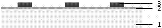
[0031] Such as figure 1 As shown, the substrate 1 is glass, the semiconductor 2 is titanium dioxide, the metal 3 is gold, the semiconductor 2 is evenly covered on the substrate 1, and the metal 3 sheet-like micro-nano structure is on the semiconductor 2 to form a metal-semiconductor composite micro-nano structure . The structure can be prepared by the following steps: uniformly deposit a layer of titanium dioxide film on the glass substrate, spin-coat a layer of photoresist on it, and use multi-beam interference exposure technology (or nanosphere lithography technology) on the photoresist A periodic micro-nano structure is formed on it, and a layer of gold film is sputtered (or evaporated) on it, and the gold film on the photoresist is removed by a lift-off process, while the gold in the gap of the photoresist micro-nano structure in contact with the titanium dioxide film is retained. thin film, thereby forming a gold sheet-like micro-nano structure, forming a gold-titanium d...

Embodiment 2

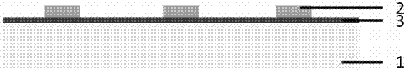
[0034] Such as figure 2As shown, the substrate 1 is glass, the semiconductor 2 is titanium dioxide, the metal 3 is gold, the metal 3 is evenly covered on the substrate 1, and the semiconductor 2 sheet-like micro-nano structure is on the metal 3 to form a metal-semiconductor composite micro-nano structure . The structure can be prepared by the following steps: uniformly deposit a layer of gold film on the glass substrate, spin-coat a layer of photoresist on it, and use multi-beam interference exposure technology (or nanosphere lithography technology) on the photoresist Form a periodic micro-nano structure on it, sputter (or evaporate) a layer of titanium dioxide film on it, use the stripping process to remove the titanium dioxide film on the photoresist, and keep the titanium dioxide in the gap of the photoresist micro-nano structure in contact with the gold film thin film, thereby forming a titanium dioxide flake micro-nano structure, and forming a gold-titania composite mic...

Embodiment 3

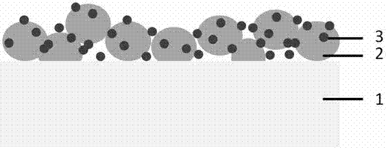
[0037] Such as image 3 As shown, the substrate 1 is silicon, the semiconductor 2 is titanium dioxide, the metal 3 is gold, the semiconductor 2 is nanospheres, and the metal 3 is nanospheres. structure. The structure can be prepared by the following steps: chemically synthesize gold nanospheres and titanium dioxide nanospheres, uniformly mix the two to form a suspension of gold nanospheres and titanium dioxide nanospheres, and spin coat, scrape, or spray the suspension Evenly distributed on the silicon substrate, after drying, a gold-titanium dioxide composite micro-nano structure can be formed.

[0038] Those skilled in the art can modify and adjust on the basis of Embodiment 3, for example, the substrate 1 can be replaced by transparent flexible substrates such as polyethylene terephthalate (PET) plastics, transparent rigid substrates such as glass, or It can be replaced by flexible and rigid substrates with micro-nano structures on the surface. Semiconductor 2 can be repl...


PUM


Abstract

The invention discloses a visible light-near infrared band solid state photocatalytic purifying film apparatus which comprises a substrate, a semiconductor and a metal. The metal and the semiconductor are in contact and are in contact with air and form a metal-semiconductor compound micro-nano structure; and the metal-semiconductor compound micro-nano structure is located on the substrate. Compared with a conventional photocatalytic purifying device based on wide band-gap semiconductor nanoparticles, the visible light-near infrared band solid state photocatalytic purifying film apparatus disclosed by the invention based on the metal-semiconductor compound micro-nano structure can expand a catalytic response band to a visible light-infrared band, so that the utilization efficiency of light sources such as sunlight and an indoor fluorescent lamp can be greatly increased; moreover, the visible light-near infrared band solid state photocatalytic purifying film apparatus is free of loss and secondary pollution, so that the visible light-near infrared band solid state photocatalytic purifying film apparatus is more stable, safe and environmental-friendly.

Description

technical field [0001] The invention belongs to the technical field of photocatalysis, and specifically relates to a visible light-near-infrared band solid-state photocatalytic purification device based on a metal-semiconductor composite micro-nano structure. Background technique [0002] Photocatalytic technology is a green technology with important application prospects in the fields of energy and environment. It has been applied in wastewater treatment, air purification and the preparation of superhydrophilic materials. [0003] Existing photocatalytic purification products mostly use wide-bandgap semiconductors (such as titanium dioxide) as catalysts. Only under the irradiation of high-energy photons (such as ultraviolet light) can the valence band electrons of the catalyst rise to the conduction band and form holes in the valence band. Therefore, it has a strong photocatalytic ability. Since the ultraviolet portion of sunlight is very weak, the photocatalytic ability o...

Claims


Application Information

Patent Timeline
Patent Type & Authority Applications(China)
IPC IPC(8): B01D53/86B01D53/44B81B1/00
CPCB01D53/8687B81B1/00B01D2255/20707B01D2255/106B01D2255/104B01D2255/20761B01D2259/80B01D2259/802B01D2255/802
Inventor 何赛灵杨柳
Owner SUZHOU YOUHAN INFORMATION TECH CO LTD
Why Eureka
Try Eureka