Manufacturing process for improving capacity of aluminum gallium indium phosphorus light-emitting diodes

A light-emitting diode, gallium indium phosphide technology, applied in the field of quaternary light-emitting diodes, can solve the problems of reducing single-chip production, and achieve the effects of improving yield, reducing cracking, and reducing costs

Active Publication Date: 2010-10-13
ANHUI SANAN OPTOELECTRONICS CO LTD
View PDF1 Cites 32 Cited by
  • Summary
  • Abstract
  • Description
  • Claims
  • Application Information

AI Technical Summary

Problems solved by technology

The invention uses the chemical etching method to completely replace the "half-cut" in the conventional process, and only needs to cut the chip twice to completely separate the core particles without touching the PN junction surface at all, avoiding hard damage to the PN junction and shortening the production process. cycle, which improves the qualified rate of the device; however, this process step is easily affected by the isotropy of wet etching, and the loss width between the core grains is as high as 20-60um, which greatly reduces the single-chip yield

Method used


Image

  • Manufacturing process for improving capacity of aluminum gallium indium phosphorus light-emitting diodes
  • Manufacturing process for improving capacity of aluminum gallium indium phosphorus light-emitting diodes
  • Manufacturing process for improving capacity of aluminum gallium indium phosphorus light-emitting diodes

Examples


Embodiment Construction

[0023] The present invention will be further described below in conjunction with the accompanying drawings and embodiments.

[0024] The manufacturing process for increasing the yield of aluminum gallium indium phosphide light-emitting diodes, the process steps are as follows:

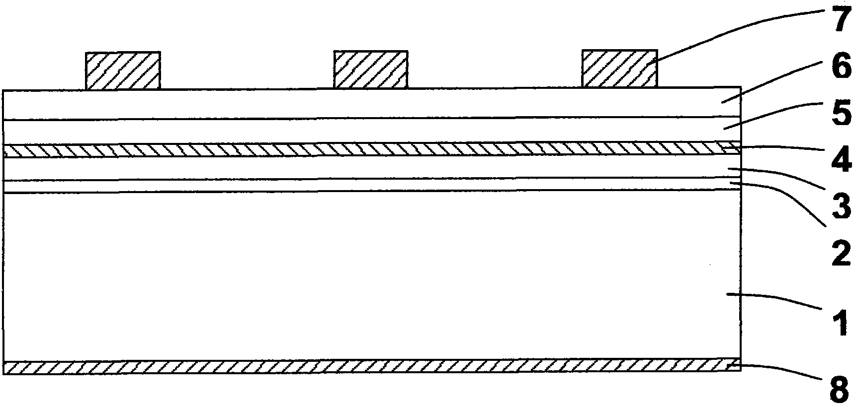
[0025] Such as figure 1 As shown, a distributed Bragg reflection layer 2, a first-type epitaxial layer 3, a light-emitting layer 4, a second-type epitaxial layer 5, and a window layer 6 are sequentially formed on a GaAs substrate 1; a P electrode 7 is formed on the window layer 6 And form an N electrode 8 on the bottom surface of the substrate 1 to form a wafer;

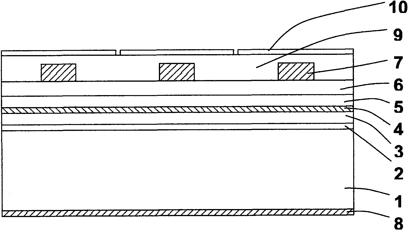
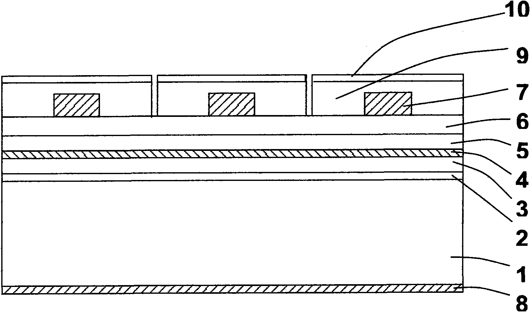
[0026] Such as figure 2 As shown, a protective layer is formed on the top surface of the wafer to cover the P electrode 7, and a 3 μm dicing line is formed on the top surface of the wafer by photolithography technology, and the size of the pre-cut grain is defined, wherein the top protective layer is made of SiO 2 The first protective la...


PUM


Abstract

The invention discloses a manufacturing process for improving the capacity of aluminum gallium indium phosphorus light-emitting diodes. After finishing conventional processes, the technical combination of dry wet etching and cleavage is adopted to replace a diamond knife cutting technology to separate core particles; the dryly etched anisotropy etching can reduce crack of core particle margin, so as to reduce area loss between core particles, can improve single-chip output amount, effectively avoid electric leakage caused by the fact that the cut residual dust attaches to side face, thus improving yield of products, and effectively reducing production cost.

Description

technical field [0001] The invention relates to a quaternary light-emitting diode, in particular to a manufacturing process for improving the production capacity of an aluminum gallium indium phosphide light-emitting diode. Background technique [0002] LEDs are mainly used in dot-matrix displays, traffic lights, indoor and outdoor display screens, automobile tail lights, etc., so they require high reliability. First, it is necessary to epitaxially grow the AlGaInP LED light-emitting structure on the GaAs substrate, and then carry out conventional cleaning, electrode fabrication, photolithography, thinning and other semiconductor processes. The electrode pattern is made on the window layer. The window layer is made of GaP material, GaAs substrate and The layers between the GaP window layers are collectively referred to as epitaxial layers. After the conventional process is completed, testing is required to ensure that the brightness, wavelength, voltage, reverse leakage cur...

Claims


Application Information

Patent Timeline
Patent Type & Authority Applications(China)
IPC IPC(8): H01L33/00H01L21/78
Inventor 林素慧蔡家豪张美林科闯
Owner ANHUI SANAN OPTOELECTRONICS CO LTD
Why Eureka
Try Eureka