Semiconductor device with heat radiation and gain

A semiconductor and conductor chip technology, which is applied in semiconductor devices, semiconductor/solid-state device components, electric solid-state devices, etc., can solve problems such as labor-intensive, time-consuming and labor-intensive, laser drilling costs and time, etc., to improve design freedom The effect of high temperature, stable placement, and good heat dissipation structure

Inactive Publication Date: 2010-11-03
BRIDGE SEMICON
View PDF3 Cites 11 Cited by
  • Summary
  • Abstract
  • Description
  • Claims
  • Application Information

AI Technical Summary

Problems solved by technology

However, although this packaging structure can achieve the purpose of heat dissipation, it is only after the overall structure is completed in the processing process that laser blind holes need to be made and thermally conductive materials are filled to obtain this device with improved heat dissipation. While this technology wants to improve structural heat dissipation, it also has the disadvantage of spending additional costs and time for laser drilling and other processes, which is also time-consuming, labor-intensive and labor-intensive.

Method used


Image

  • Semiconductor device with heat radiation and gain
  • Semiconductor device with heat radiation and gain
  • Semiconductor device with heat radiation and gain

Examples


Embodiment Construction

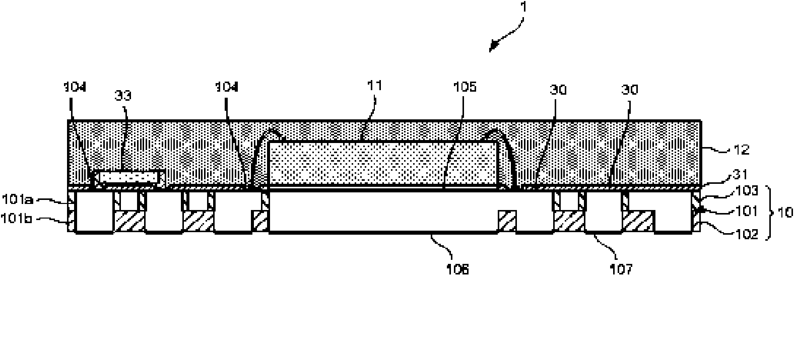
[0088] see figure 1 Shown is a schematic cross-sectional view of the semiconductor device according to the first preferred embodiment of the present invention. As shown in the figure: the present invention is a semiconductor device with heat dissipation gain, which at least includes a metal substrate 10 with a complete circuit surface and a complete pin surface, a semiconductor chip 11 and a molding material 12 .

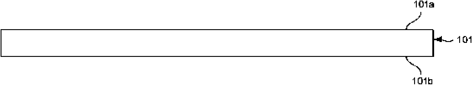
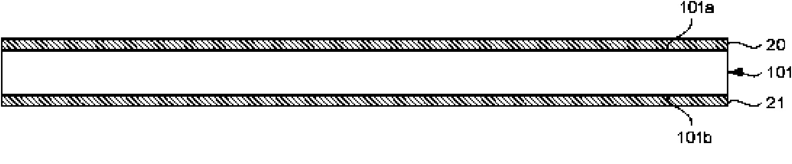
[0089] The metal substrate 10 includes a metal plate 101 , a first insulating layer 102 and a second insulating layer 103 . Wherein the metal plate 101 includes an upper portion 101a and a lower portion 101b relative to the upper portion, and the upper portion 101a of the metal plate 101 includes a crystal pad area and a plurality of patterned circuit areas, and the second insulating layer 103 is It is arranged between the patterned circuit areas and the crystal pad area; the lower part 101b of the metal plate 101 includes an electrical pad area connected to the c...


PUM


Abstract

The invention relates to a semiconductor device with heat radiation and gain, comprising an integrated metal base board comprising an etching circuit, a dielectric material, a thick copper-placed crystal heat-radiation bonding pad and a plurality of electric pin bonding pads. The semiconductor device is characterized in that a chip can be directly combined with the thick copper-placed crystal heat-radiation bonding pad so that a favorable heat-radiation structure is provided when the chip is operated; and in addition, because the integrated metal base board in the semiconductor device has the dielectric material, the etching circuit can be supported to be independent of the electric pin bonding pads, the semiconductor device can improve design freedom and allow the wiring of finer circuits to strengthen coiling required when electronic assemblies are connected. Meanwhile, because the circuit is supported by the dielectric material, an anti-welding layer can be formed on the circuit to stably place welding assemblies. The invention can effectively solve the problems of poor heat radiation of the traditional packaging plastic base board, insufficient coiling capacity of a lead frame, bad electricity caused by no placement of the welding assemblies and the like.

Description

technical field [0001] The present invention relates to a semiconductor device with heat dissipation gain, especially a semiconductor device that can improve the problems of poor heat dissipation of traditional packaging plastic substrates, insufficient winding capacity of lead frames, and poor electrical performance due to no function of placing soldered components. Background technique [0002] With the continuous development of semiconductor technology, the chips carried by semiconductor devices tend to be highly integrated to provide the operation speed and functions required by electronic products. However, at the same time, the heat generated by the operation of the chips also increases relatively. In the past, lead frame packaging was generally used. Although a good heat dissipation effect can be obtained by using lead frame packaging, it does not have the ability to route fine lines. Another solution is to use a plastic substrate to obtain good winding capability, bu...

Claims


Application Information

Patent Timeline
Patent Type & Authority Applications(China)
IPC IPC(8): H01L23/14H01L23/48H01L23/482H01L23/29
CPCH01L2924/19105H01L2224/48091H01L2224/73265H01L2224/32245H01L2224/48247H01L24/73H01L2924/181
Inventor 陈振重王家忠林文强
Owner BRIDGE SEMICON
Why Eureka
Try Eureka