

Copper foil provided with carrier
A technology of copper foil with carrier and copper foil carrier, applied in the manufacture of printed circuit precursors, printed circuit manufacturing, metal pattern materials, etc., can solve the problems of residual copper particles, poor insulation of circuit patterns, etc.
- Summary
- Abstract
- Description
- Claims
- Application Information
AI Technical Summary
Problems solved by technology
Method used
Image

Examples
Embodiment
[0273] Hereinafter, the present invention will be described in more detail through examples of the present invention, but the present invention is not limited by these examples.
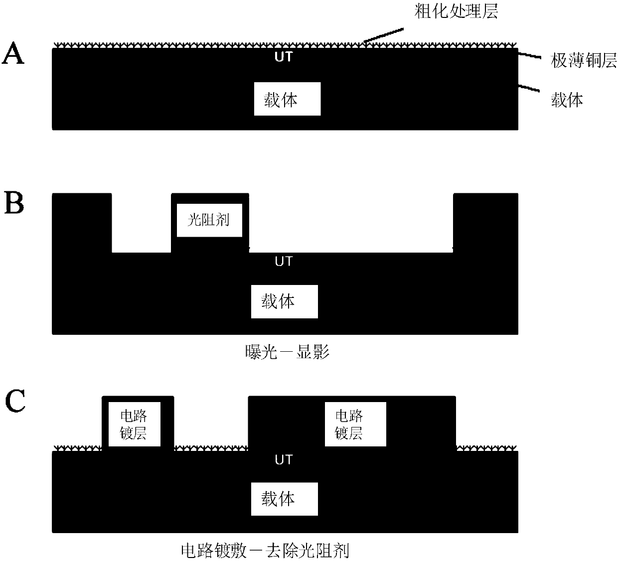
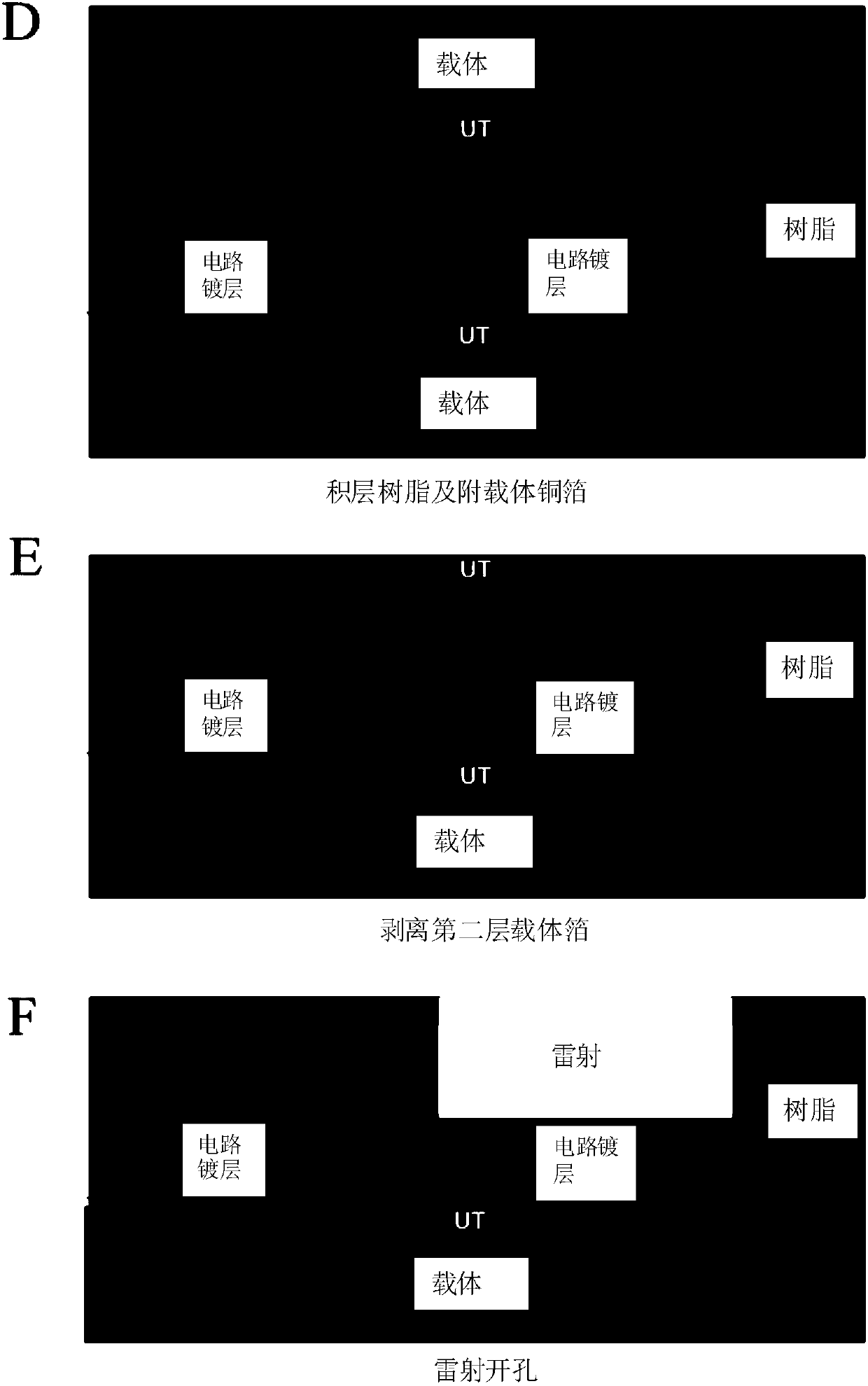
[0274] 1. Manufacture of copper foil with carrier
[0275]
[0276] As a copper foil carrier, a 35-micrometer-thick long electrolytic copper foil (JTC manufactured by JX Nippon Oil Metal Co., Ltd.) was prepared. The glossy surface of the copper foil was electroplated using a roll-to-roll continuous plating line under the following conditions, thereby forming 4000 μg / dm 2 The amount of Ni layer attached.
[0277] ·Ni layer
[0278] Nickel sulfate: 250~300g / L
[0279] Nickel chloride: 35~45g / L
[0280] Nickel acetate: 10~20g / L
[0281] Trisodium citrate: 15~30g / L
[0282] Gloss agent: saccharin, butynediol, etc.
[0283] Sodium lauryl sulfate: 30~100ppm
[0284] pH: 4~6
[0285] Bath temperature: 50~70℃
[0286] Current density: 3~15A / dm 2
[0287] After washing with water and pickling, 1...
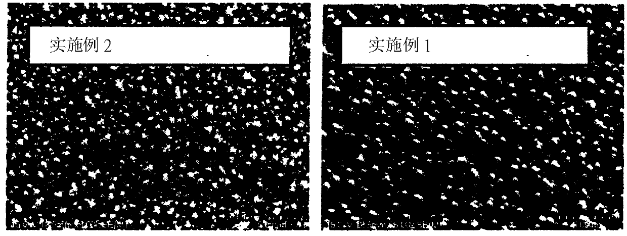
Embodiment 2
[0345] After forming an ultra-thin copper layer on the copper foil carrier under the same conditions as in Example 1, the following roughening treatment 1, roughening treatment 2, antirust treatment, chromate treatment, and silane coupling treatment were performed in sequence. In addition, the thickness of the ultra-thin copper foil was set to 3 μm.
[0346] ·Coarsening treatment 1
[0347] Liquid composition: copper 10-20g / L, sulfuric acid 50-100g / L
[0348] Liquid temperature: 25~50℃
[0349] Current density: 1~58A / dm 2
[0350] Coulomb quantity: 4~81As / dm 2
[0351] ·Coarsening 2
[0352] Liquid composition: copper 10~20g / L, nickel 5~15g / L, cobalt 5~15g / L
[0353] pH: 2~3
[0354] Liquid temperature: 30~50℃
[0355] Current density: 24~50A / dm 2
[0356] Coulomb quantity: 34~48As / dm 2
[0357] ·Anti-rust treatment
[0358] Liquid composition: nickel 5~20g / L, cobalt 1~8g / L
[0359] pH: 2~3
[0360] Liquid temperature: 40~60℃
[0361] Current density: 5~20A / dm ...
Embodiment 3
[0372] After forming an ultra-thin copper layer on the copper foil carrier under the same conditions as in Example 1, the following roughening treatment 1, roughening treatment 2, anti-rust treatment, and chromate treatment were sequentially performed on the surface of the ultra-thin copper layer. treatment, and silane coupling treatment. In addition, the thickness of the ultra-thin copper foil was set to 3 μm.
[0373] ·Coarsening treatment 1
[0374] (liquid composition 1)
[0375] Cu: 10~30g / L
[0376] h 2 SO 4 : 10~150g / L
[0377] As: 0~200mg / L
[0378] (plating condition 1)
[0379] Temperature: 30~70℃
[0380] Current density: 25~110A / dm 2
[0381] Coarse Coulomb quantity: 50~500As / dm 2
[0382] Plating time: 0.5 to 20 seconds
[0383] ·Coarsening 2
[0384] (liquid composition 2)
[0385] Cu: 20~80g / L
[0386] h 2 SO 4 : 50~200g / L
[0387] (plating condition 2)
[0388] Temperature: 30~70℃
[0389] Current density: 5~50A / dm 2
[0390] Coarse Coulo...
PUM
| Property | Measurement | Unit |
|---|---|---|
| surface roughness | aaaaa | aaaaa |
| surface roughness | aaaaa | aaaaa |
| thickness | aaaaa | aaaaa |
Abstract
Description
Claims
Application Information