TFT-LCD (Thin Film Transistor-Liquid Crystal Display) array base plate and manufacturing method thereof

A technology of an array substrate and a manufacturing method, applied in the field of a TFT-LCD array substrate and its manufacturing, can solve the problems of different degrees of undercut, cumbersome processing procedures, different degrees of inward inclination of the undercut, etc., so as to improve the yield and simplify the Technological difficulty, the effect of avoiding pollution

Active Publication Date: 2010-11-24
BOE TECH GRP CO LTD +1
View PDF0 Cites 49 Cited by
  • Summary
  • Abstract
  • Description
  • Claims
  • Application Information

AI Technical Summary

Problems solved by technology

[0012] However, after etching the second insulating layer to form the undercut of the photoresist, an ashing process of the photoresist is required, so in actual production, it is difficult to maintain the undercut of the photoresist
In addition, there will also be a problem of different degrees of undercut formation, that is, different degrees of inward inclination of the undercut, resulting in a high probability of failure during the lift-off process, resulting in a decrease in the yield
In addition, when the photoresist is ashed, it will pollute the transparent conductive layer, which will bring a very high defect rate, and also bring the corresponding cumbersome processing procedures.

Method used


Image

  • TFT-LCD (Thin Film Transistor-Liquid Crystal Display) array base plate and manufacturing method thereof
  • TFT-LCD (Thin Film Transistor-Liquid Crystal Display) array base plate and manufacturing method thereof
  • TFT-LCD (Thin Film Transistor-Liquid Crystal Display) array base plate and manufacturing method thereof

Examples


Embodiment Construction

[0041] The technical solutions of the present invention will be described in further detail below with reference to the accompanying drawings and embodiments.

[0042] It should be noted:

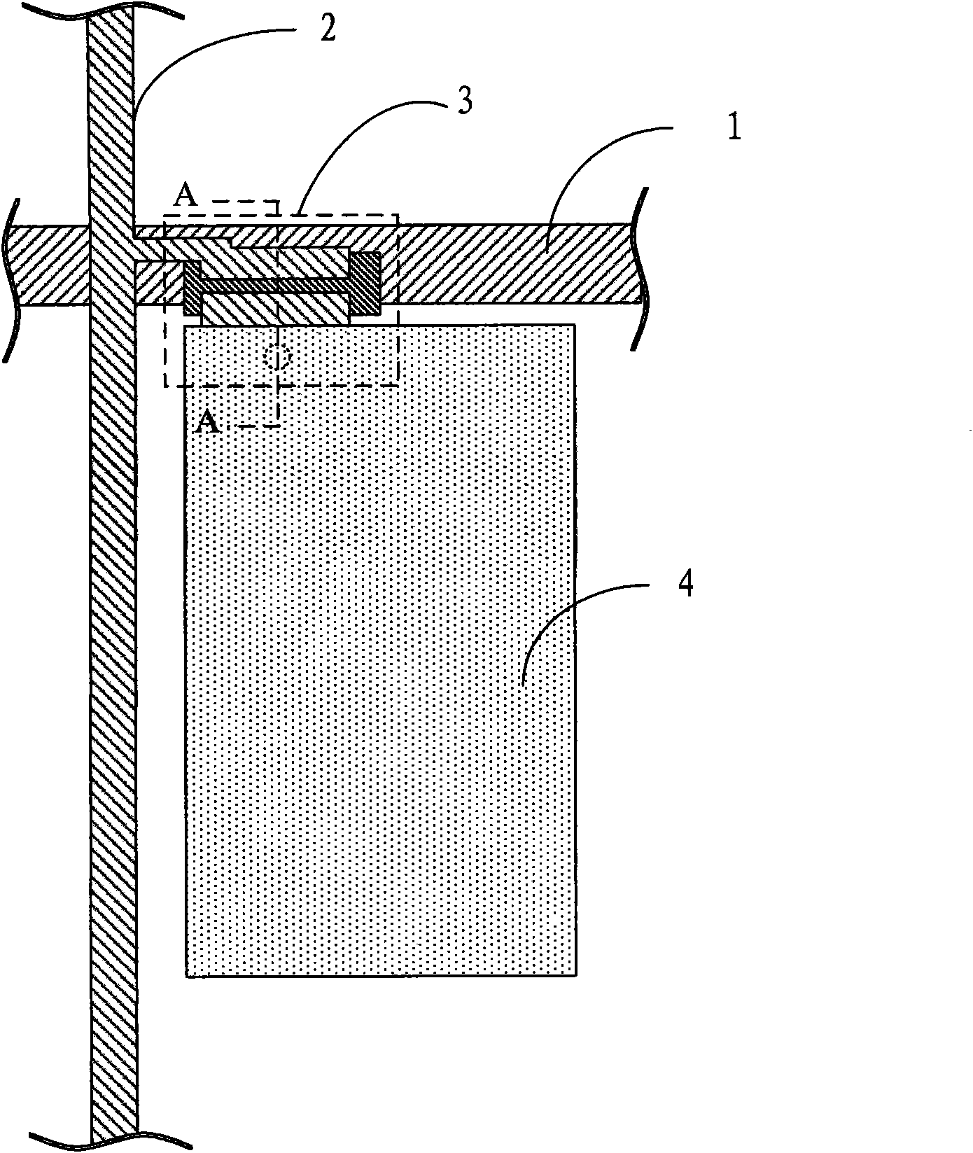
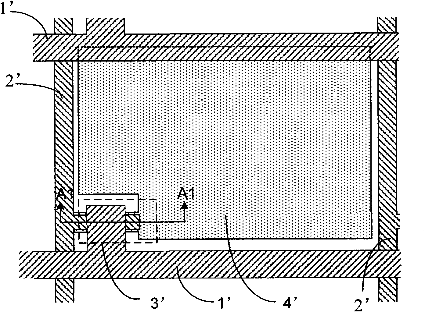
[0043] 1. In the present invention, for example, the "upper" in "X is placed on Y" includes the meaning that X is in contact with Y, and X is located above Y. In the present invention, as shown in the accompanying drawings, the transparent substrate is defined as is set at the bottom;

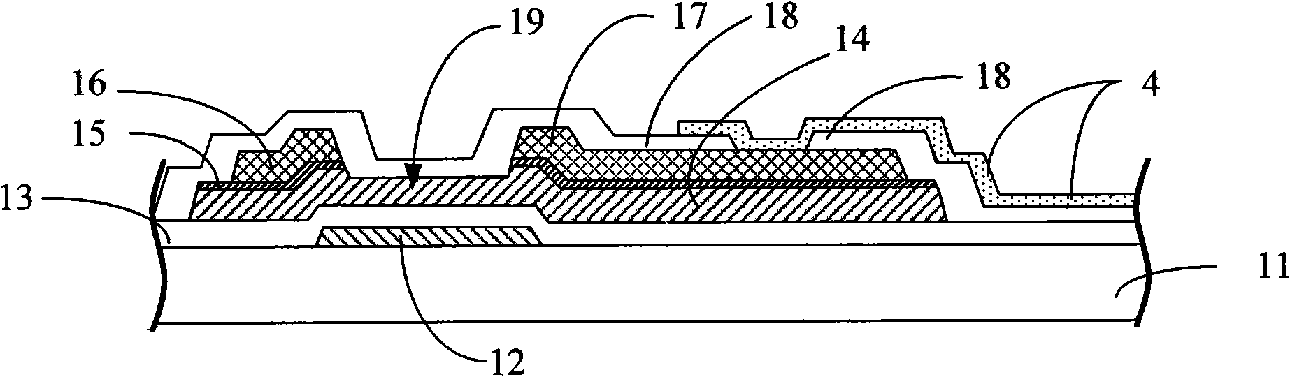
[0044]2. The patterning process referred to in the present invention includes processes such as photoresist coating, masking, exposure, development, etching, photoresist stripping, and the photoresist is an example of a positive photoresist;

[0045] 3. The "so-and-so area" mentioned in the present invention is the area where a certain figure is mapped on the transparent substrate, that is, the area has the same shape as the certain figure, such as the grid line area, that is, the figure of the grid line is...


PUM


Abstract

The invention discloses a TFT-LCD (Thin Film Transistor-Liquid Crystal Display) array base plate and a manufacturing method thereof. The manufacturing method comprises the steps of: sequentially depositing a transparent conductive thin film, a source-drain metal thin film and a doped semiconductor thin film on a transparent base plate; forming a figure which comprises a doped semiconductor layer, a source electrode, a drain electrode, a data line and a pixel electrode by a first composition process; depositing the semiconductor thin film; forming a figure which comprises a TFT channel and a semiconductor layer by a second composition process; depositing an insulating thin film and a grid metal thin film; and forming a figure which comprises a grid line and a grid electrode by a third composition process. In the invention, three composition processes are used for manufacturing the TFT-LCD array base plate with a top grid structure. Compared with the traditional three composition processes for manufacturing the array base plate, the manufacturing method of the invention does not need a lift-off peeling process, largely simplifies the process difficulty, and enhances the product yield.

Description

technical field [0001] The invention relates to a liquid crystal display and a manufacturing method thereof, in particular to a TFT-LCD array substrate and a manufacturing method thereof. Background technique [0002] A Thin Film Transistor Liquid Crystal Display (TFT-LCD for short) is a main flat panel display (FPD for short). [0003] figure 1 It is a schematic plan view of an existing TFT-LCD array substrate. Such as figure 1 As shown, an existing array substrate (Array Substrate) includes: a gate line 1 , a data line 2 , a thin film transistor (Thin Firm Transistor, TFT for short) 3 and a pixel electrode 4 . The gate lines 1 are arranged laterally on the transparent substrate 11 , the data lines 2 are arranged vertically on the transparent substrate 11 , and TFTs 3 are arranged at intersections of the gate lines 1 and the data lines 2 . TFT3 is an active switching element. [0004] figure 2 for figure 1 A-A sectional view. Such as figure 2 As shown, the existi...

Claims


Application Information

Patent Timeline
Patent Type & Authority Applications(China)
IPC IPC(8): H01L21/84H01L21/027H01L21/311H01L27/12
CPCH01L27/1288H01L27/1214
Inventor 刘圣烈崔承镇宋泳锡
Owner BOE TECH GRP CO LTD
Why Eureka
Try Eureka