Method for manufacturing printed wiring board

A technology for printed wiring boards and wiring patterns, which is applied in the manufacture of printed circuit precursors, printed circuits, printed circuit manufacturing, etc. It can solve the problems of difficult positioning and positioning in the photolithography process, and achieve the effect of high productivity

Inactive Publication Date: 2010-11-24
UBE IND LTD
View PDF2 Cites 7 Cited by
  • Summary
  • Abstract
  • Description
  • Claims
  • Application Information

AI Technical Summary

Problems solved by technology

[0005] However, if the metal layer is further thinned to pursue a finer pitch, the wet spray process tends to cause stretching in the substrate material, and if non-uniform stretching occurs in one direction, in some cases, Positioning in the photolithography process and positioning of internal leads and bumps in the semiconductor chip mounting process will become difficult

Method used


Image

  • Method for manufacturing printed wiring board
  • Method for manufacturing printed wiring board
  • Method for manufacturing printed wiring board

Examples


Embodiment 1

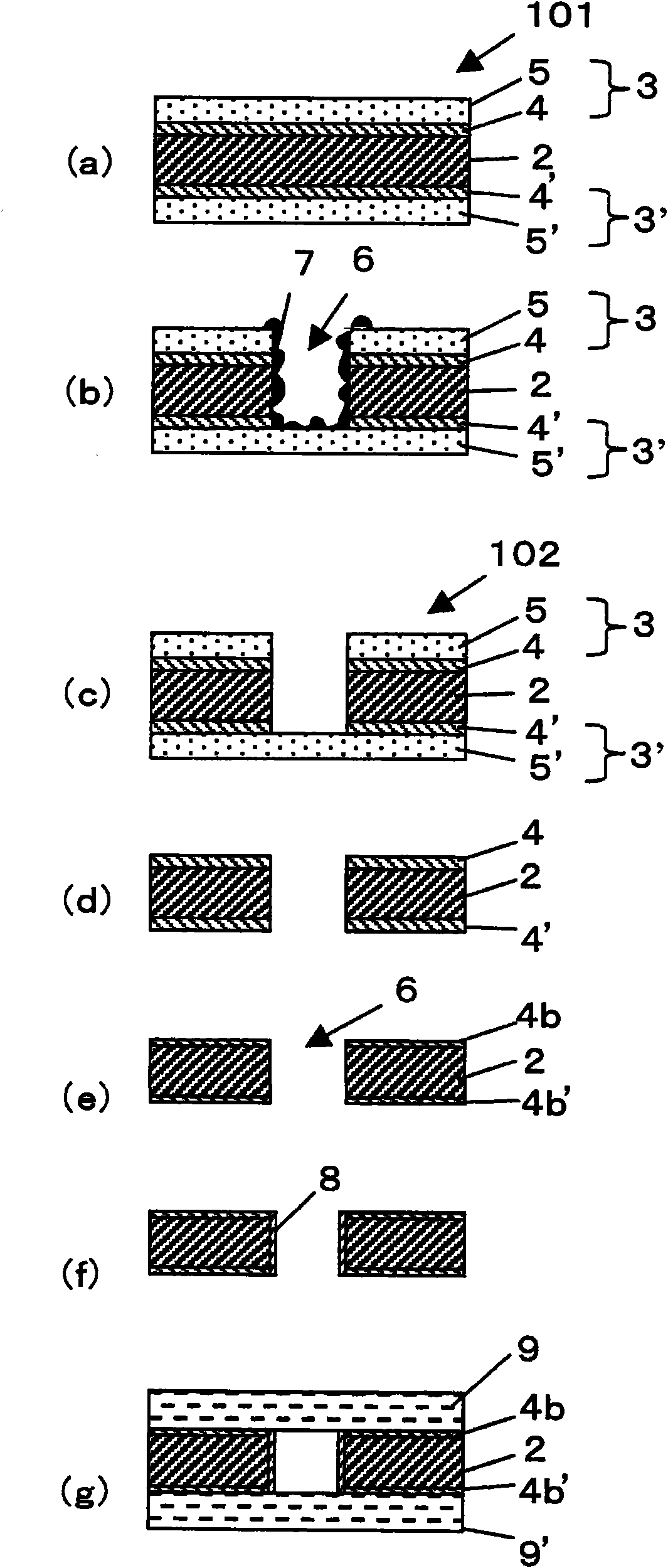
[0088] In this example, Figure 1A and 1B An example of a method of forming a circuit by a semi-additive method using a polyimide film on both sides of which a copper foil sheet with a carrier is laminated is exemplified in .

[0089] Such as Figure 1A As shown in (a), there is provided a polyimide film 101 on both sides of which a copper foil sheet with a carrier is laminated. This double-sided copper foil laminated polyimide film 101 with a carrier includes a copper foil 3 with a carrier, a polyimide film 2 and a copper foil 3' with a carrier laminated in this order, each of which has a carrier The copper foils (3, 3') are laminated layers of respective copper foils (4, 4') and carrier foils (5, 5') as protective layers. Here, the thickness of the copper foil is in the range of 1 to 8 μm, preferably in the range of 1 to 6 μm.

[0090] In the next step, as Figure 1A Shown in (b), utilize the copper foil 3 that has carrier, polyimide film 2 and copper foil 4 ' on one si...

Embodiment 2

[0106] In this example, Figure 2A and 2B exemplifies a process example of forming a circuit by a semi-additive method using a polyimide film laminated with a copper foil sheet with a carrier on both sides.

[0107] Such as Figure 2A As shown in (a), there is provided a polyimide film 101 laminated with copper foil with a carrier on both sides. In this double-sided copper foil laminated polyimide film with carrier 101, copper foil 3 with carrier, polyimide film 2, and copper foil 3' with carrier are laminated in this order, with carrier The copper foils (3, 3') are laminates of copper foils (4, 4') and carrier foils (5, 5'), where the thickness of the copper foils ranges from 1 to 8 μm, preferably from 1 to 8 μm. 6 μm.

[0108] In the next step, as Figure 2A As shown in (b), a through hole is formed at a predetermined position of the double-sided copper foil laminated polyimide film 101 with a carrier through the copper foil 3 with a carrier and the polyimide film 2 on ...

Embodiment 3

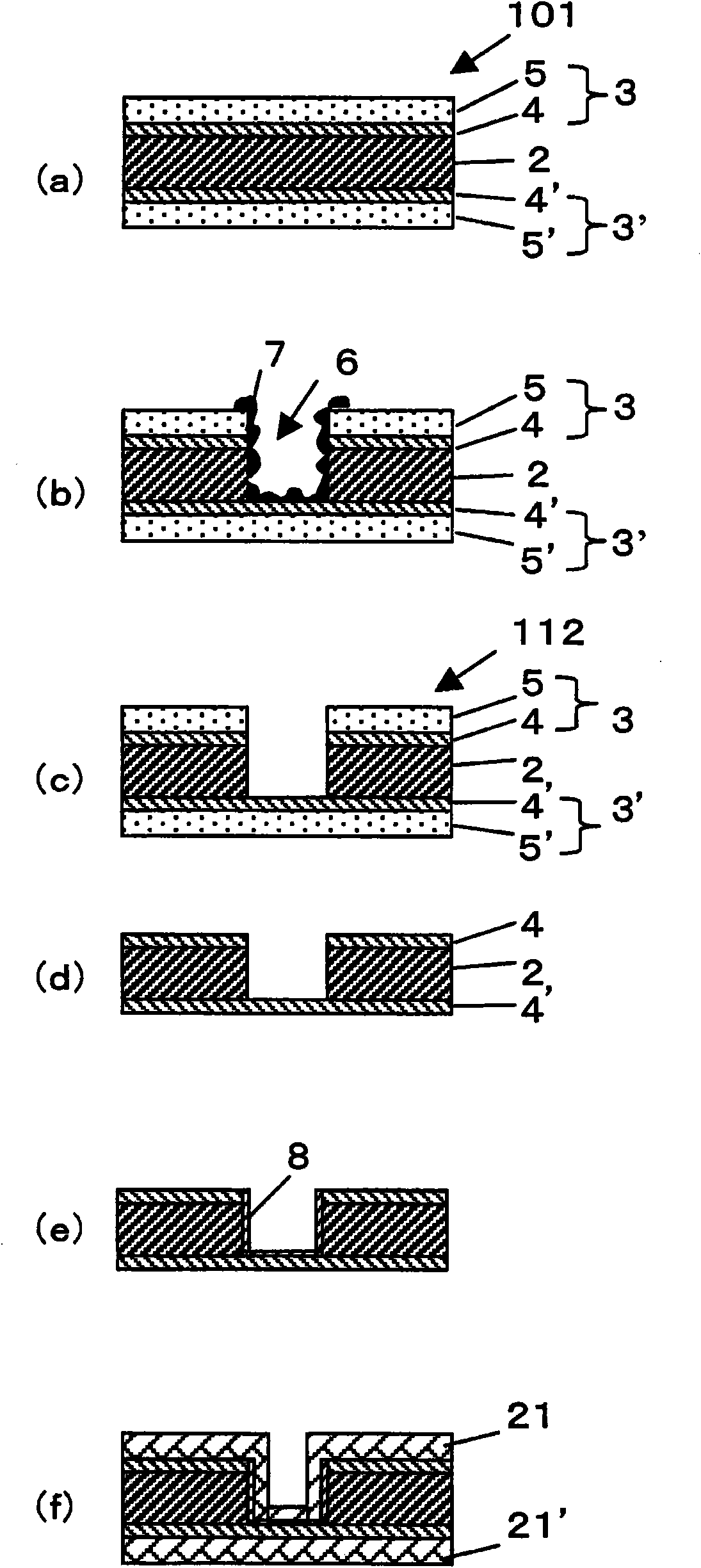
[0118] In this example, image 3 An example of a method of forming a via hole in the via hole forming process of Embodiments 1 and 2 is illustrated.

[0119] Such as image 3 As shown in (a), there is provided a polyimide film 101 on both sides of which a copper foil sheet with a carrier is laminated. This double-sided copper foil laminated polyimide film 101 with a carrier includes a copper foil 3 with a carrier, a polyimide film 2 and a copper foil 3' with a carrier, each of which has a copper foil with a carrier Foils (3, 3') are laminates of respective copper foils (4, 4') and carrier foils (5, 5') as protective layers, the copper foils having a thickness in the range of 1 to 8 μm, preferably in the range of 1 to 6 μm.

[0120] In the next step, as image 3 As shown in (b), utilize laser etc. to pass through copper foil 3 and 3 ' both sides with carrier and polyimide film 2, form on a part of double-sided copper foil laminated polyimide film 101 with carrier Through h...


PUM


Abstract

Provided is a method for manufacturing with high productivity a printed wiring board having high dimensional stability. The manufacturing method is provided with a step of preparing a metallic laminated body wherein a metal layer having an inner metal layer section and a protection layer section is laminated on at least one side of an insulating resin layer, with the inner metal layer section on the side of the insulating resin layer; a step of forming a via hole on the metal layer and the insulating resin layer; a step of performing blast processing after forming the via hole; and a step of removing the protection layer section after performing blast processing.

Description

technical field [0001] The present invention relates to a method of manufacturing a printed wiring board having through holes. Background technique [0002] Since copper foil laminated polyimide film has excellent characteristics such as thin thickness and light weight, it has been applied to high-performance electronic devices, specifically, it has been applied to devices with high density suitable for size reduction and weight reduction. Flexible printed circuit boards (FPC) for wiring, tape automated bonding (TAB), etc. Due to high-density integration and refinement of electronic devices, wiring boards are required to respond to high-density assembly. Double-sided wiring boards and multilayer wiring boards have been proposed as wiring boards responding to high-density mounting. In order to manufacture such double-sided and multilayer wiring boards, it is necessary to form via holes with high productivity. [0003] In general, after the step of forming a via hole, it is...

Claims


Application Information

Patent Timeline
Patent Type & Authority Applications(China)
IPC IPC(8): H05K3/40H05K3/00H05K3/26
CPCH05K2203/0361H05K2203/025H05K3/421H05K2203/1388H05K3/0055H05K2203/1383H05K3/025H05K3/427
Inventor 番场啓太横沢伊裕渡辺英明
Owner UBE IND LTD
Why Eureka
Try Eureka