

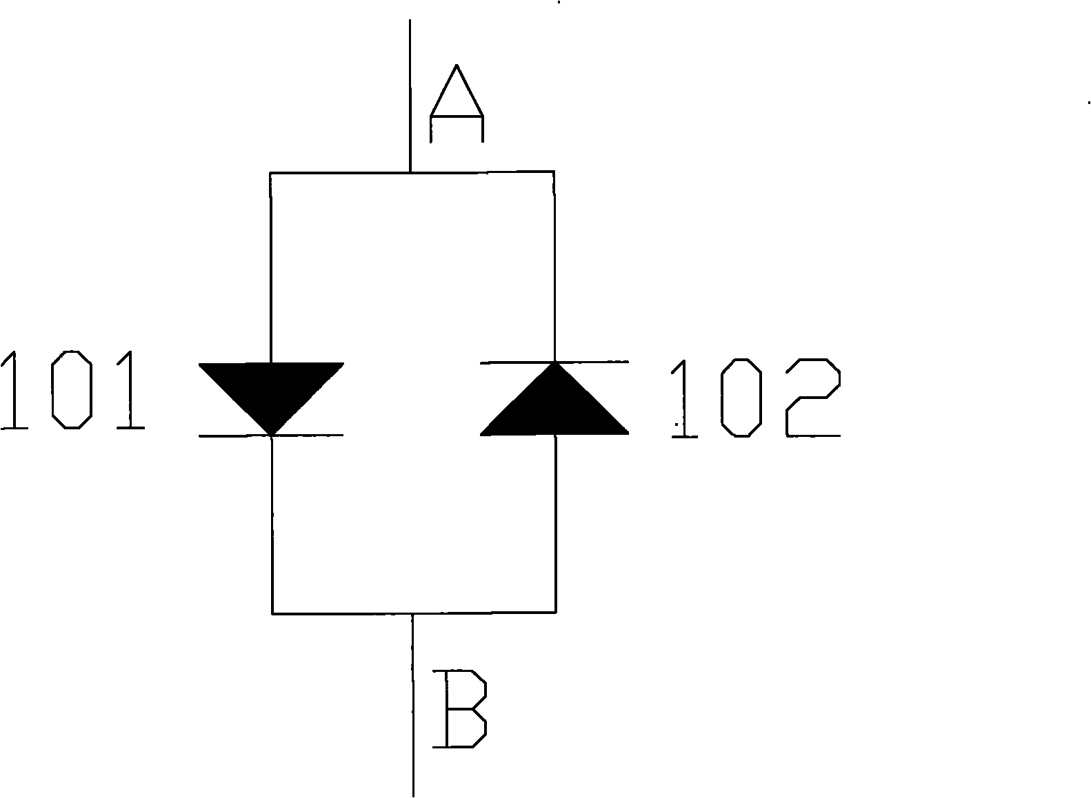
Antistatic gallium nitride based luminescent device and manufacturing method thereof
A light-emitting device, gallium nitride-based technology, applied in the direction of electrical solid-state devices, semiconductor/solid-state device manufacturing, electrical components, etc., can solve the problems of high price, large lattice mismatch, and poor machining performance of silicon carbide. Achieve the effect of simplifying the production process and improving product yield
- Summary
- Abstract
- Description
- Claims
- Application Information
AI Technical Summary
Problems solved by technology
Method used
Image

Examples
Embodiment Construction
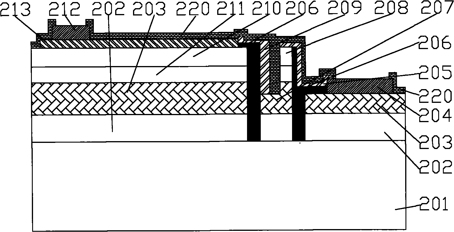
[0031] A method for manufacturing an antistatic gallium nitride-based light-emitting device, the specific steps of which are:
[0032] Step 1: growing an epitaxial buffer layer 202, an N-type gallium nitride layer 203, a multi-quantum hydrazine layer 211, and a P-type gallium nitride layer 209 (210) sequentially on a sapphire substrate 201;
[0033] Step 2: Etching part of the epitaxial layer to the depth of the sapphire substrate to completely isolate the epitaxial layer of the protective diode and the light-emitting diode; this step can be removed by ICP etching or wet etching. The epitaxial layer between the protective diode and the light-emitting diode;
[0034] Step 3: Simultaneously etching part of the epitaxial layer on the N-type gallium nitride layer by ICP or RIE in the area of the light-emitting diode and the protection diode;
[0035] Step 4: growing a transparent conductive layer 213 on the P-type gallium nitride epitaxy in the light emitting diode region;
[0...
PUM
 Abstract
Description
Claims
Application Information