Design method for transmission lines using meta-materials

A metamaterial and transmission line technology, applied in waveguide-type devices, electrical components, waveguides, etc., to solve problems affecting semiconductor circuit design

Active Publication Date: 2010-12-15
TAIWAN SEMICON MFG CO LTD
View PDF3 Cites 29 Cited by
  • Summary
  • Abstract
  • Description
  • Claims
  • Application Information

AI Technical Summary

Problems solved by technology

Therefore, the above-mentioned problems seriously affect the design of semiconducto

Method used


Image

  • Design method for transmission lines using meta-materials
  • Design method for transmission lines using meta-materials
  • Design method for transmission lines using meta-materials

Examples


Embodiment Construction

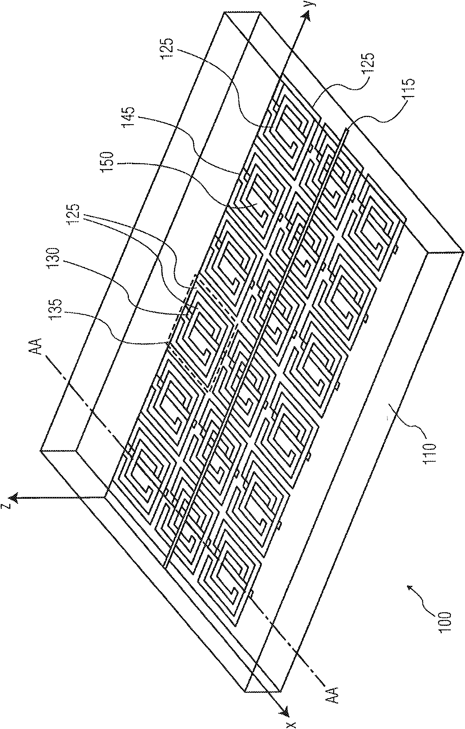
[0029] Specific embodiments described below relate to the design of transmission lines for signals in circuits or substrates by using metamaterials as insulators for the circuits or substrates. By metamaterial is meant a material designed such that the signal behaves in such a way that the shape of the signal behaves as if its permittivity and permeability differs from that of the used The real part of an insulator has a similar permittivity and permeability. It should be noted that both relative permittivity and relative permeability include real and imaginary parts, namely ε R =ε R +jε R and μ R =μ R +jμ R . Thus, metamaterials can be designed to have a signal that responds as if the permittivity and permeability had negative values. In the present invention, the insulating material is designed to reduce the noise generated by the resonance mode of the signal line. A metamaterial is an arrangement of conductors in an insulator to reduce the resonant response of a tra...


PUM


Abstract

High frequency circuits for wireless, digital and microwave applications place requirements upon the impedance of their signal lines, interconnects and packaging. In designing and implementing the substrates for these signal lines it is beneficial to employ meta-materials to provide the desired impedance. Such meta-materials providing a means to provide modified permittivity and permeability for the substrate, these being different than the real permittivity and permeability of the insulator used. In an example embodiment, a substrate is configured as a meta-material. It is desirable therefore to have a means to model these meta-material aspects of the signal lines rapidly and accurately allowing the circuits, interconnects and packages to be designed and implemented without expensive andexhaustive iterative experimental characterization. Within the cited invention design parameters for the meta-material structure are determined in dependence upon input parameters characterising the conductive medium, dielectric medium enveloping the conductive material, and the pre-determined shapes of the conductive medium.

Description

technical field [0001] The present invention relates to microwave transmission lines, and in particular to the design of transmission lines on a substrate and added with metamaterials. Background technique [0002] The electronics industry continues to rely on the development of semiconductor technology to achieve higher performance components in smaller areas. In order to achieve higher performance components in many applications, it is necessary to integrate a large number of electronic components into a single semiconductor chip. As the number of electronic components in a given area of ​​a wafer increases, the manufacturing process becomes more difficult. [0003] Various semiconductor elements have been manufactured for various applications in various disciplines. These semiconductor components generally include metal-oxide-semiconductor field-effect transistors (MOSFETs), such as P-channel metal-oxide-semiconductor field-effect transistors (PMOS), N-channel metal-oxi...

Claims


Application Information

Patent Timeline
IPC IPC(8): H01P3/08
CPCH01L2924/19051H01L2924/0002H01P3/08H01L23/66H01L2924/3011H01L2924/00
Inventor 克里斯多夫·韦蓝德
Owner TAIWAN SEMICON MFG CO LTD
Why Eureka
Try Eureka