Direct writing method for in situ reduction metal nano-structure

A metal nanostructure and in-situ technology, which is applied in the field of in-situ reduction of metal nanostructures and direct writing of in-situ reduction of metal nanostructures, can solve the problems of high cost, low efficiency, and few types of materials, and achieve high repeatable manufacturing accuracy , simple process and high manufacturing efficiency

Inactive Publication Date: 2010-12-22
XI AN JIAOTONG UNIV
View PDF1 Cites 17 Cited by
  • Summary
  • Abstract
  • Description
  • Claims
  • Application Information

AI Technical Summary

Problems solved by technology

However, these existing methods not only can process fewer ty

Method used


Image

  • Direct writing method for in situ reduction metal nano-structure
  • Direct writing method for in situ reduction metal nano-structure
  • Direct writing method for in situ reduction metal nano-structure

Examples


Example Embodiment

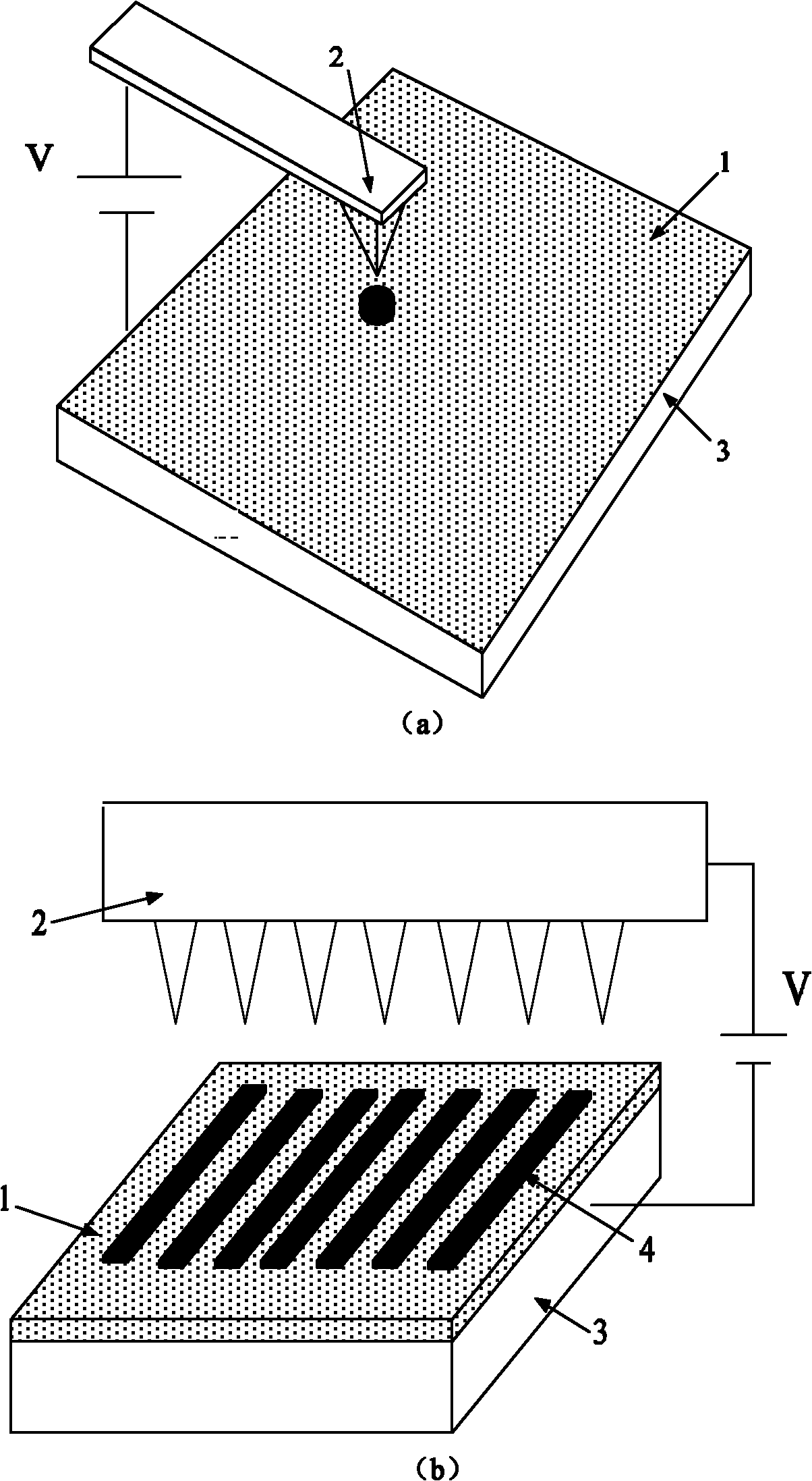
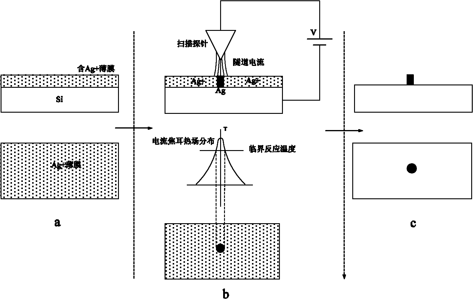
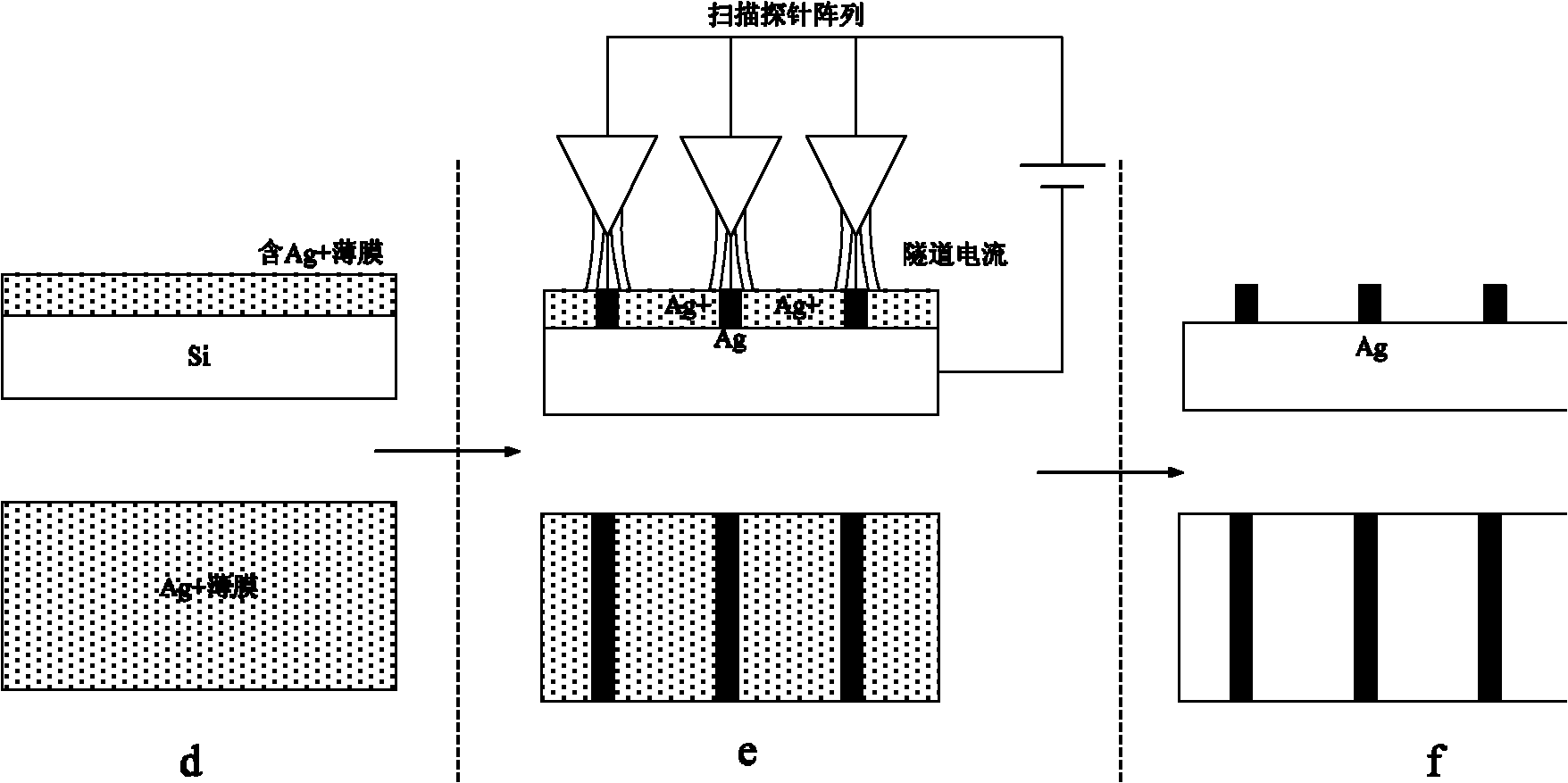
[0019] Example 2: AgNO with a mass ratio of 85:11 3 And CH 3 CHO is dissolved in ammonia water to make a mixed solution with a concentration of 252g / L, and the quartz plate is selected as the substrate 3, and the made AgNO 3 With CH 3 The ammonia solution of CHO is coated on the surface of the substrate to form a mixed solution film 1 with a thickness of 200nm; the scanning voltage of the STM scanning tunnel microscope is 10V, the electric pulse frequency is 100Hz, and the speed of the scanning probe 2 is 80nm / s.

Example Embodiment

[0020] Example 3: AgNO with a mass ratio of 85:11 3 And CH 3 CHO is dissolved in ammonia water to make a mixed solution with a concentration of 252g / L, and the quartz plate is selected as the substrate 3, and the made AgNO 3 With CH 3 The ammonia solution of CHO is coated on the surface of the substrate to form a mixed solution film 1 with a thickness of 500 nm; the scanning voltage of the STM scanning tunnel microscope is 30V, the electric pulse frequency is 500 Hz, and the scanning probe 2 speed is 50 nm / s.

Example Embodiment

[0021] Example 4: AgNO with a mass ratio of 85:11 3 And CH 3 CHO is dissolved in ammonia water to make a mixed solution with a concentration of 252g / L, and the quartz plate is selected as the substrate 3, and the made AgNO 3 With CH 3 The ammonia solution of CHO is coated on the surface of the substrate to form a mixed solution film 1 with a thickness of 800nm; the scanning voltage of the STM scanning tunnel microscope is 40V, the electric pulse frequency is 1000Hz, and the scanning probe 2 speed is 0nm / s (that is, its Stand still) to form dot-like nanostructures.


PUM

PropertyMeasurementUnit
Thicknessaaaaaaaaaa

Abstract

The invention discloses a direct writing method for in situ reduction metal nano-structure, which utilizes the property that the majority of metal ions can undergo reduction reaction under thermal catalysis condition, induces the reduction reaction of the metal ions by using the current joule heat between an STM scanning probe and a substrate to obtain metal atoms which are subjected to in-situ deposition, and directly obtains the nano-structure from the substrate surface. The principle is as follows: when an STM is used for scanning and imaging, the tunnel current between the probe and the sample surface generates current joule heat in the local micro-area of the sample when flowing through the sample, the reduction reaction of the oxidized metal ion thin layer is induced in the presence of reducing agent, and the meal ions are reduced into the metal atoms which are subjected to in-situ deposition on the substrate surface to form the metal nano-structure. The manufacturing precision of the method can reach nano level, the process is simple, the probe does not need to be pre-treated or soaked many times, continuous operation can be performed, no specific requirement is imposed on the operation environment, the size of the nano-structure is adjustable, and a complex nano-structure shape can be manufactured, therefore the method is a novel nano-processing process based on a scanning probe.

Description

technical field [0001] The invention belongs to the field of nanostructure manufacture, and relates to an in-situ reduction metal nanostructure, in particular to a direct writing method for in-situ reduction of the metal nanostructure. Background technique [0002] With the rapid development of nanotechnology, its application has spread across many technical fields such as information, biology, energy, environment, and machinery. In recent years, the feature size of nano-devices has become smaller and smaller, while their functions have become more powerful. The rapid advancement of the nanometer scale to below 50nm also poses new challenges to the nanostructure manufacturing technology. At present, the nano-manufacturing processes and methods of 50nm and below include direct electron beam etching, focused ion beam FIB etching, extreme ultraviolet lithography EUV, nanoimprinting, scanning probe microscope processing and other process methods. However, these existing method...

Claims


Application Information

Patent Timeline
IPC IPC(8): B22F9/24
Inventor 段玉岗丁玉成刘芬芬张小辉卢秉恒
Owner XI AN JIAOTONG UNIV
Why Eureka
Try Eureka