C/X dual-band microstrip antenna

A microstrip antenna and C-band technology, which is applied in antennas, antenna arrays, antenna grounding devices, etc., can solve problems such as large crosstalk, decreased mechanical reliability, and process errors, so as to improve output power and gain, increase coupling, and reduce The effect of small disturbances

Inactive Publication Date: 2010-12-29
UNIV OF ELECTRONIC SCI & TECH OF CHINA
View PDF1 Cites 29 Cited by
  • Summary
  • Abstract
  • Description
  • Claims
  • Application Information

AI Technical Summary

Problems solved by technology

However, due to the double-layer structure of the antenna, process errors are introduced, and the mechanical reliabilit

Method used


Image

  • C/X dual-band microstrip antenna
  • C/X dual-band microstrip antenna
  • C/X dual-band microstrip antenna

Examples


Embodiment Construction

[0035] specific implementation plan

[0036] The present invention will be further described below:

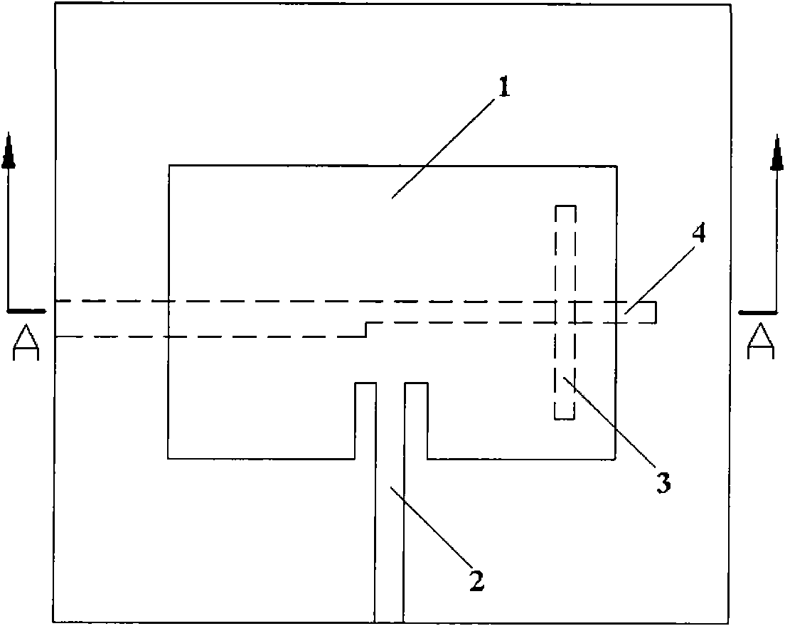
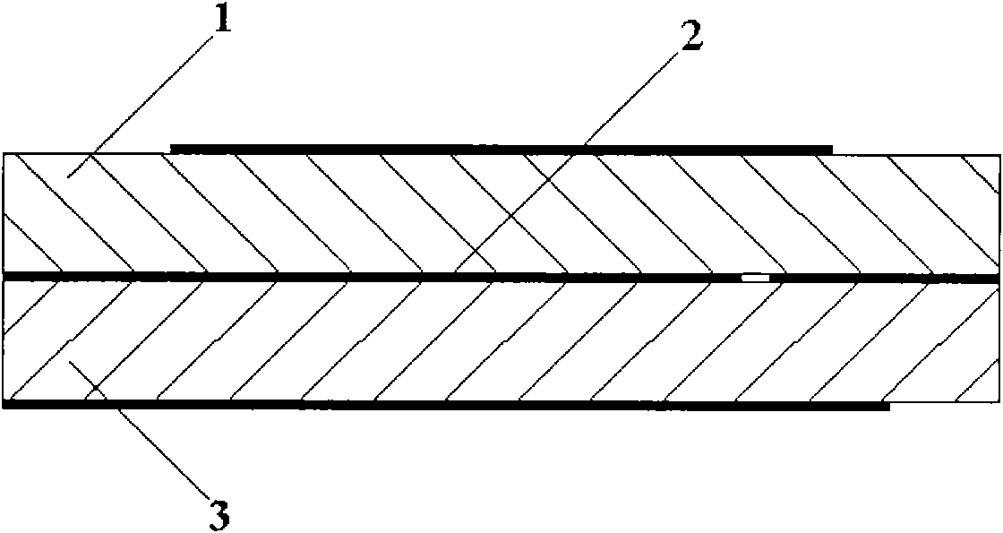
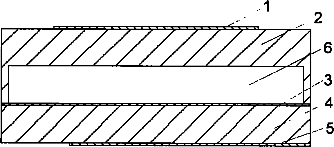
[0037] 1. The higher the dielectric constant of the dielectric substrate, the smaller the antenna size, the larger the half-power beam width, and the worse the bandwidth and efficiency. In order to integrate with radio frequency devices such as circuits or MEMS switches, high-dielectric constant silicon is used as the medium. At this time, the bandwidth of the conventionally designed microstrip antenna cannot meet the design requirements, and the efficiency is also very low. There is a contradiction between miniaturization and large bandwidth. In this case, an air cavity with an appropriate thickness is dug out at the bottom of the silicon substrate to reduce the composite dielectric constant to achieve miniaturization, light weight and broadband requirements. Therefore, this antenna uses high-resistance silicon (relative permittivity of 11.9, electrical conductivity of 0.033...


PUM


Abstract

The invention discloses a C/X dual-band microstrip antenna, and belongs to the technical field of antennas. The antenna adopts a dual-layer high-resistance silicon medium structure in which two frequency bands share a rectangular radiation patch; an upper layer of high-resistance silicon media bears a rectangular patch and an X frequency band feed line; an air cavity is etched on an upper layer of high-resistance silicon to reduce a composite dielectric constant of the high-resistance silicon; a lower layer of high-resistance media bear a C frequency band feed line; an X frequency band adopts microstrip coplanar feeding; and a C frequency band adopts slot coupling feeding. The C/X dual-band microstrip antenna or a C/X dual-band two-element microstrip antenna has the following advantages of: 1, singlechip and dual modes, simple structure and flexible design; 2, multiple frequencies; 3, miniaturization and light weight; and 4, integration. The C/X dual-band microstrip antenna can be widely applied to airborne point-to-point communication tools, such as satellite communications, control, guide and radars.

Description

technical field [0001] The invention belongs to the technical field of antennas, and relates to a C / X dual-band microstrip patch antenna for point-to-point communication in the air. Background technique [0002] Air communication node technology, involving aircraft, satellites and other carriers. With the continuous development of digital technology, network technology, system technology, and MEMS technology, the air communication node technology has undergone major changes. The overall technical development requirement is to reduce the weight of the equipment, that is, to reduce the volume, weight and power consumption. Using digital technology, software technology, MEMS technology, high-density assembly technology, etc. to realize the multi-functional integration of air communication node equipment is an inevitable trend to meet the needs of modern communication. [0003] In the past, air communication node equipment was bulky and heavy, and had high requirements for air...

Claims


Application Information

Patent Timeline
IPC IPC(8): H01Q1/38H01Q1/48H01Q5/01H01Q13/08H01Q21/00H01Q5/10
Inventor 刘晓明魏景辉
Owner UNIV OF ELECTRONIC SCI & TECH OF CHINA
Why Eureka
Try Eureka