
Ytterbium/bismuth dual-doped lead tungstate crystal and preparation method thereof

A lead tungstate, double doping technology, applied in crystal growth, chemical instruments and methods, single crystal growth, etc.

Active Publication Date: 2011-01-05
SHANGHAI INST OF CERAMIC CHEM & TECH CHINESE ACAD OF SCI
View PDF10 Cites 5 Cited by
  • Summary
  • Abstract
  • Description
  • Claims
  • Application Information

AI Technical Summary

Problems solved by technology

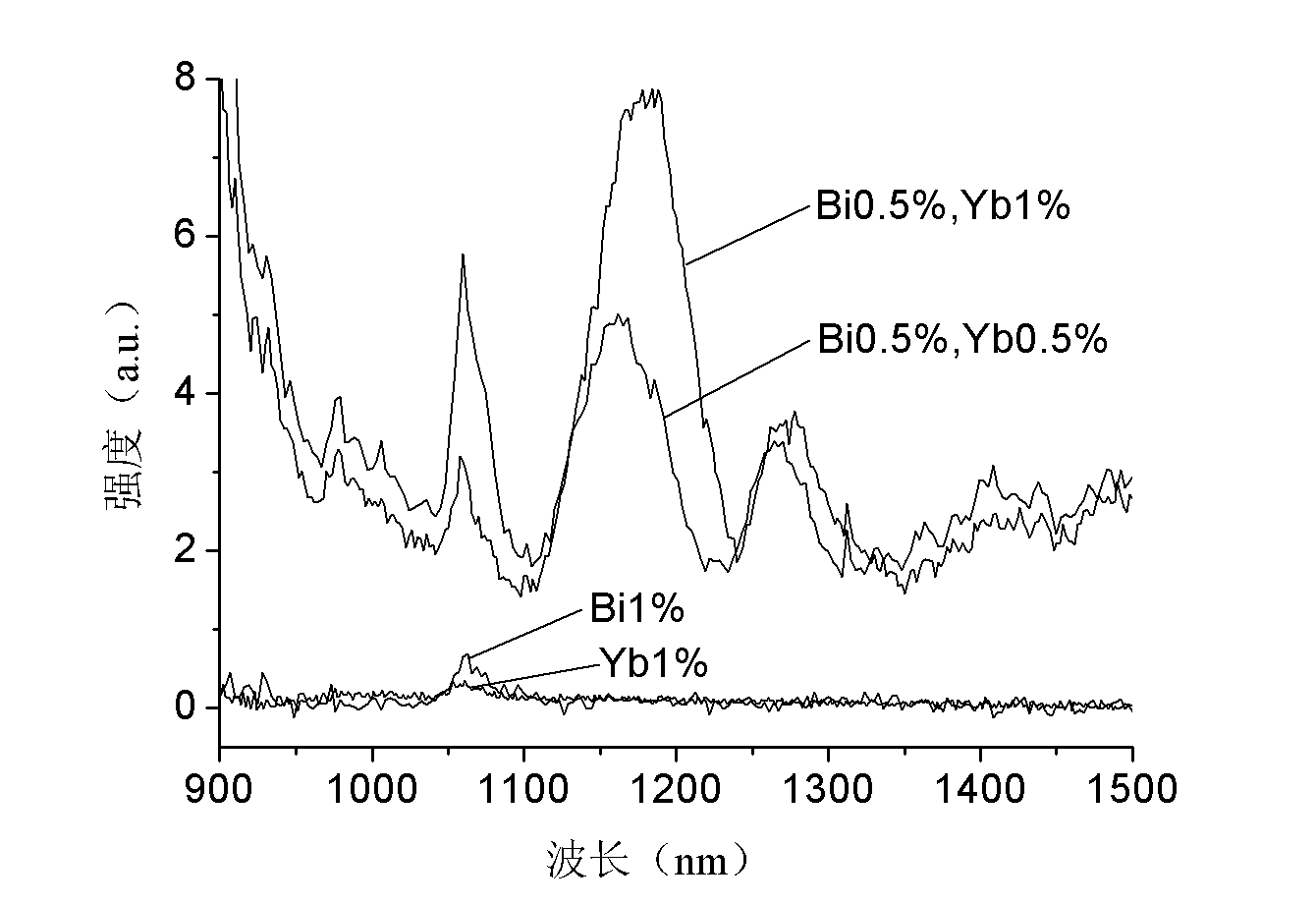
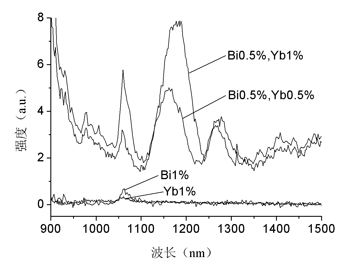
At present, there is no consensus on the luminescence mechanism of Bi ions. Many scholars believe that the near-infrared luminescence center should be attributed to the low-valence state Bi. n+ Ions (n=0, 1, 2), usually by chemical reduction or γ-ray irradiation to make normal Bi 3+ The ion is reduced to the low-valence state Bi n+ ions to produce near-infrared luminescence, and the current research results show that none of the above methods can make single-doped Bi 3+ Ionic PWO crystals generate near-infrared luminescence

Method used


Image

  • Ytterbium/bismuth dual-doped lead tungstate crystal and preparation method thereof
  • Ytterbium/bismuth dual-doped lead tungstate crystal and preparation method thereof

Examples


Embodiment 1

[0023] 1. Combine high-purity PbO and WO with a purity of 99.99% 3 The powder is precisely proportioned according to the stoichiometric ratio, and is melted in a platinum crucible to make a high-density PWO polycrystalline ingot;

[0024] 2. A Φ20×200mm crucible is made of single-layer platinum with a thickness of 0.14mm;

[0025] 3. The PWO single crystal with an orientation of and a size of Φ18×55mm is used as the seed crystal;

[0026] 4. With high purity Bi 2 o 3 Incorporate PWO polycrystalline material as dopant, Bi 3+ The doping amount is 1.0 at%, the growth raw material is put into the platinum crucible, and finally the seed crystal is put in and the crucible is closed, and the crystal growth is carried out by the descending method;

[0027] 5. Put the platinum crucible into the downcomer, raise the furnace temperature to 1230°C after 12 hours, then keep it warm for about 4 hours, and then gradually lift the downcomer to gradually melt the raw materials in the cruc...

Embodiment 2

[0030] 1, process step is with step 1 in embodiment 1;

[0031] 2. A crucible of 15×15×150mm is made of single-layer platinum with a thickness of 0.14mm;

[0032] 3. The PWO single crystal with an orientation of and a size of 13×13×50mm is used as a seed crystal;

[0033] 4. With high purity Yb 2 o 3 Incorporate PWO polycrystalline material as dopant, Yb 3+ The doping amount is 1.0 at%, and the growth raw material is put into the platinum crucible, and finally the seed crystal is put in and the crucible is closed, and the crystal growth is carried out by the descending method;

[0034] 5. Put the platinum crucible into the downcomer, raise the furnace temperature to 1250°C after 15 hours, then keep it warm for about 6 hours, and then gradually lift the downcomer to gradually melt the raw materials in the crucible until they are all melted Keep warm for 2 hours, at this time, crystal growth can be carried out, and the downcomer is lowered at a rate of 1.2mm / h;

[0035] 6....

Embodiment 3

[0037] 1, process step is with step 1-3 in embodiment 1;

[0038] 2. With high purity Bi 2 o 3 and Yb 2 o 3 Doping the PWO polycrystalline material as a dopant, where Bi 3+ The doping amount is 1.0at%, Yb 3+The doping amount is 1.0 at%, the growth raw material is put into the platinum crucible, and finally the seed crystal is put in and the crucible is closed, and the crystal growth is carried out by the descending method;

[0039] 3. The process steps are the same as steps 5-6 in Example 2.


PUM

PropertyMeasurementUnit
Thicknessaaaaaaaaaa

Abstract

The invention relates to an Yb<3+> / Bi<3+> dual-doped lead tungstate crystal and a preparation method thereof, and belongs to the field of optical crystals. Bi ions in the PWO crystal generate multiband near-infrared luminescence through energy transfer between Yb<3+> and Bi <n+> (n is equal to 0, 1 and 2) under the sensitization of the Yb<3+> ions. The Yb<3+> / Bi<3+> dual-doped lead tungstate crystal is prepared by mixing Bi2O3 and Yb2O3 powder into a lead tungstate polycrystalline ingot by a Czochralski method and a crucible descending method, wherein the doping amount of Bi<3+> in the obtained crystal is between 0.1 and 2.0 atom percent, and the doping amount of the Yb<3+> is between 0.3 and 4.0 atom percent.

Description

technical field [0001] The present invention relates to a kind of Yb 3+ / Bi 3+ A double-doped lead tungstate crystal and a preparation method thereof belong to the field of optical crystals. technical background [0002] Lead tungstate (PbWO 4 , referred to as PWO) is a new type of scintillation crystal, which is widely used in high-energy physics, nuclear medicine and other fields because of its high density, fast decay, high irradiation hardness, and low cost. In addition, PWO crystals also have the characteristics of wide light transmission range, stable physical and chemical properties, high thermal conductivity and high damage threshold, and have obvious advantages in the application of laser crystals. [0003] Near-infrared luminescent materials with main group metal ions Bi as active ions are emerging research hotspots in recent years. The broadband near-infrared luminescence produced can be used to realize wide-wavelength tuning and ultrashort pulse laser output. ...

Claims


Application Information

Patent Timeline
IPC IPC(8): C30B29/32C30B11/00C30B15/00
Inventor 熊巍袁晖陈良周尧
Owner SHANGHAI INST OF CERAMIC CHEM & TECH CHINESE ACAD OF SCI
Learn More