Method for repairing broken circuit or mutilation of copper bonding pad and repair structure thereof

An incomplete and brazing technology, which is applied in the field of circuit break repair of printed circuit boards, can solve problems such as non-solderability, poor appearance quality of printed circuit boards, contact, etc., and achieve fast results

Active Publication Date: 2012-05-23
福州瑞华印制线路板有限公司
View PDF0 Cites 0 Cited by
  • Summary
  • Abstract
  • Description
  • Claims
  • Application Information

AI Technical Summary

Problems solved by technology

[0002] There will be 1%-2% wire circuit boards in the reproduction process of printed circuit boards. Two methods can be used to repair such circuit boards. One is to use ordinary pressure welding to repair wire circuit breaks. There are three defects in this type of pressure welding. : 1. The solder joints are only on two pressure soldering points, resulting in no practical contact between the repaired copper wire and the substrate at the gap of the printed circuit board; 2. The open circuit with a large span cannot be repaired, only the small opening can be repaired Broken lines and straight line broken lines, large-area wire breaks and bend wire breaks are helpless, and copper pad open circuits and via hole open circuits cannot be repaired; 3. The appearance quality of the repaired printed board is poor
However, this chemical method cannot repair the defects of the copper pad, and it is not solderable after repair

Method used


Image

  • Method for repairing broken circuit or mutilation of copper bonding pad and repair structure thereof
  • Method for repairing broken circuit or mutilation of copper bonding pad and repair structure thereof
  • Method for repairing broken circuit or mutilation of copper bonding pad and repair structure thereof

Examples


Embodiment Construction

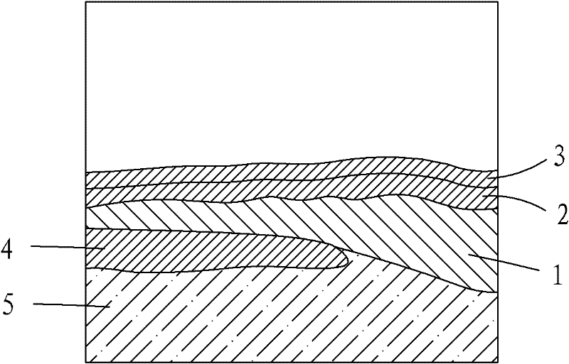
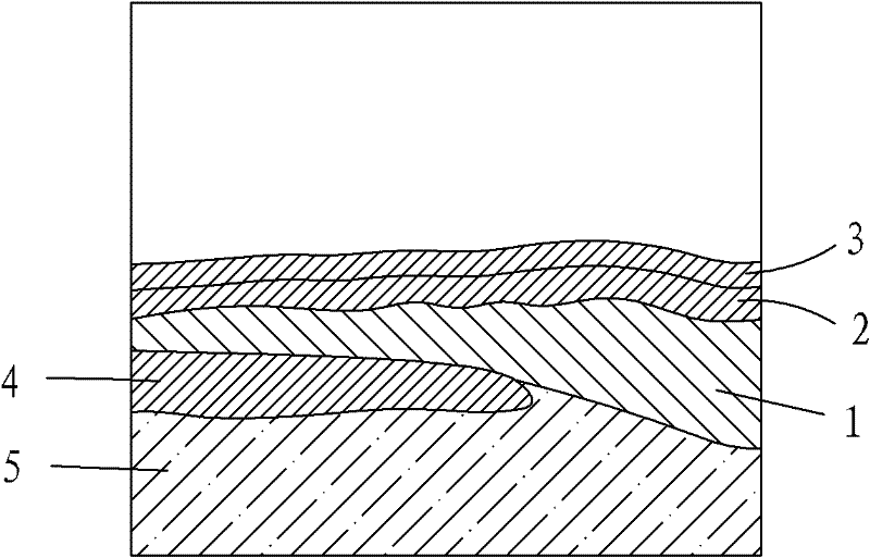
[0023] See 1 and figure 2 , to describe the embodiment of the present invention in more detail.

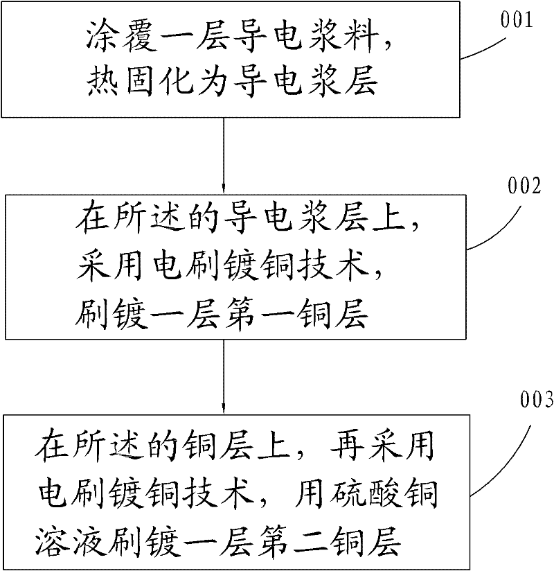
[0024] Such as figure 1 , is a flow chart of a copper pad disconnection or incomplete repair method of the present invention. The first step is to first coat a layer of conductive paste accounting for 1 / 3 of the total repair thickness on the copper pad wire disconnection position or incomplete part as the base layer, the conductive paste is silver paste, and the silver paste After being baked, it is thermally cured into a silver paste layer, and this layer of silver paste layer is used as the basis for the conductive layer and subsequent repairs. In the second step, on the silver paste layer, a layer of first copper layer is brush-plated. The first copper layer is an electroplating potion using copper nitrate solution, and a layer of copper layer is brush-plated. The first copper layer accounts for about 1 / 3 of the total repair thickness. In the third step, on the basis of t...


PUM


Abstract

The invention provides a method for repairing a broken circuit or the mutilation of a copper bonding pad, which is based on the technology of conductive paste bottoming and electric brush copper plating. The method comprises the following steps of: 1, coating a layer of conductive paste at the position which is needed to be repaired, and thermocuring the conductive paste to form a conductive paste layer; 2, performing brush plating on the conductive paste layer by adopting the technology of electric brush plating to form a first copper layer; and 3, performing the brush plating on the first copper layer by adopting copper sulfate solution to form a second copper layer. A repair structure adopting the repair method comprises the conductive paste layer, the first copper layer and the second copper layer formed by the electric brush plating of the copper sulfate solution from inside to outside, wherein the first copper layer is a copper layer formed by the electric brush plating of copper nitrate solution. Through the repair method and the repair structure, the problem of the common pressure welding method is solved, and the outer surface of the copper bonding pad has weldability.

Description

【Technical field】 [0001] The invention relates to a technique for repairing a circuit break of a printed circuit board, in particular to a method for repairing a circuit break or defect of a copper pad and its structure. 【Background technique】 [0002] There will be 1%-2% wire circuit boards in the reproduction process of printed circuit boards. Two methods can be used to repair such circuit boards. One is to use ordinary pressure welding to repair wire circuit breaks. There are three defects in this type of pressure welding. : 1. The solder joints are only on two pressure soldering points, resulting in no practical contact between the repaired copper wire and the substrate at the gap of the printed circuit board; 2. The open circuit with a large span cannot be repaired, only the small opening can be repaired Broken wires and straight line wires, large-area wire wire breaks and bend wire wire wire wire breaks are helpless, and copper pad open circuits and via hole open circu...

Claims


Application Information

Patent Timeline
Patent Type & Authority Patents(China)
IPC IPC(8): H05K3/10H05K3/24H05K1/02
Inventor 许秀恋陈跃生何华辉
Owner 福州瑞华印制线路板有限公司
Why Eureka
Try Eureka