Framework of high speed and low power consumption serial communication data receiving interface

A serial communication and receiving interface technology, which is applied in the field of high-speed and low-power serial communication data receiving interface architecture, can solve problems affecting the image quality of image sensors, etc., and achieve the effects of reducing power consumption, reducing production costs, and reducing requirements

Inactive Publication Date: 2011-01-19
昆山芯视讯电子科技有限公司
View PDF0 Cites 8 Cited by
  • Summary
  • Abstract
  • Description
  • Claims
  • Application Information

AI Technical Summary

Problems solved by technology

[0009] For example, the general-purpose USB2.0 physical layer (PHY) implemented using such an architecture consumes about 60mA of current at high speed, which is not a big...

Method used


Image

  • Framework of high speed and low power consumption serial communication data receiving interface
  • Framework of high speed and low power consumption serial communication data receiving interface
  • Framework of high speed and low power consumption serial communication data receiving interface

Examples


Embodiment Construction

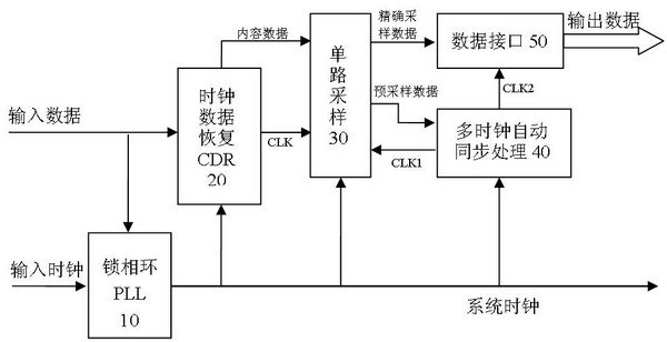
[0031] The following is attached figure 2 The specific implementation manner of the high-speed and low-power serial communication data receiving interface architecture of the present invention is described.

[0032] First, an input clock received from the outside passes through a phase-locked loop (PLL) 10 to generate a system clock with the highest frequency of the system. The phase-locked loop (PLL) 10 is a phase feedback automatic control module with functions of clock synchronization and phase locking. It implements frequency multiplication of the input clock by locking the phase to obtain the system clock synchronized with the input data. The synchronized system clocks are respectively output to the clock data recovery module (CDR) 20, the single-channel sampling module 30 and the multi-clock automatic processing module in the present invention.

[0033] The above input data is also connected to the open-loop clock data recovery module (CDR) 20, the clock data recovery ...


PUM


Abstract

The invention relates to a framework of a high speed and low power consumption serial communication data receiving interface, which discards the arrangement of a multi-channel oversampling and arbitration circuit. Through utilizing the technology of combining single-channel sampling asynchronization and multiple-clock automatic synchronization, an original clock frequency signal CLK is extracted from input data, and content data are pre-sampled; and after the pre-sampling data and a system clock are synchronized, a clock CLK1 is fed back and adjusted to a single-channel sampling module so that a result of precisely sampling the content data is completely synchronous to a target clock CLK2, thereby realizing the combination of clock domain asynchronization and synchronization and improving the efficiency. Under the condition of the similar realization area of an ASIC (Application Specific Integrated Circuit), the power consumption of realizing a physical layer (PHY) is reduced by more than 70% and exceeds the international level achieved by the traditional realization framework, thereby reducing the interference of a high speed signal on other circuits inside an ASIC chip, lowering the requirements for the layout and the wiring of a module inside the chip, reducing the energy consumption and also lowering the production cost.

Description

technical field [0001] The invention relates to an integrated circuit design and implementation, in particular to a high-speed and low-power serial communication data receiving interface architecture. Background technique [0002] With the rapid development of modern digital communication technology, interconnection technology with a rate above 5Gbit / s is being more and more widely used, such as high-speed backplane of communication system, interconnection between backplanes of communication system, local area network, very short distance between communication equipment Optical interconnection (VSR), SATA high-speed transmission standard, Express PCI2.0 and USB3.0 protocol, etc. These interconnection methods often require the support of high-speed, low-power, and cheap integrated circuits to achieve higher performance-cost ratios. [0003] The above-mentioned high-speed digital communication systems generally transmit data in a serial manner, but do not provide a dedicated ...

Claims


Application Information

Patent Timeline
IPC IPC(8): G06F13/38
CPCY02B60/1235Y02B60/1228Y02D10/00
Inventor 职春星周正伟吴钰淳
Owner 昆山芯视讯电子科技有限公司
Why Eureka
Try Eureka