Method for overcoming defects of silicon chip with STI and method for constructing STI on silicon chip

A technology for silicon wafers and structures is applied in the field of suppressing defects in silicon wafers with shallow trench isolation trench structures, and can solve problems such as affecting the performance of semiconductor circuits and irregular surface defects.

Inactive Publication Date: 2011-01-26
SEMICON MFG INT (SHANGHAI) CORP +1
View PDF0 Cites 2 Cited by
  • Summary
  • Abstract
  • Description
  • Claims
  • Application Information

AI Technical Summary

Problems solved by technology

In addition, irregular surface defects also appear on the surface of the silicon substrate 101 near the corner region 102
The aforemen

Method used


Image

  • Method for overcoming defects of silicon chip with STI and method for constructing STI on silicon chip
  • Method for overcoming defects of silicon chip with STI and method for constructing STI on silicon chip
  • Method for overcoming defects of silicon chip with STI and method for constructing STI on silicon chip

Examples


Embodiment Construction

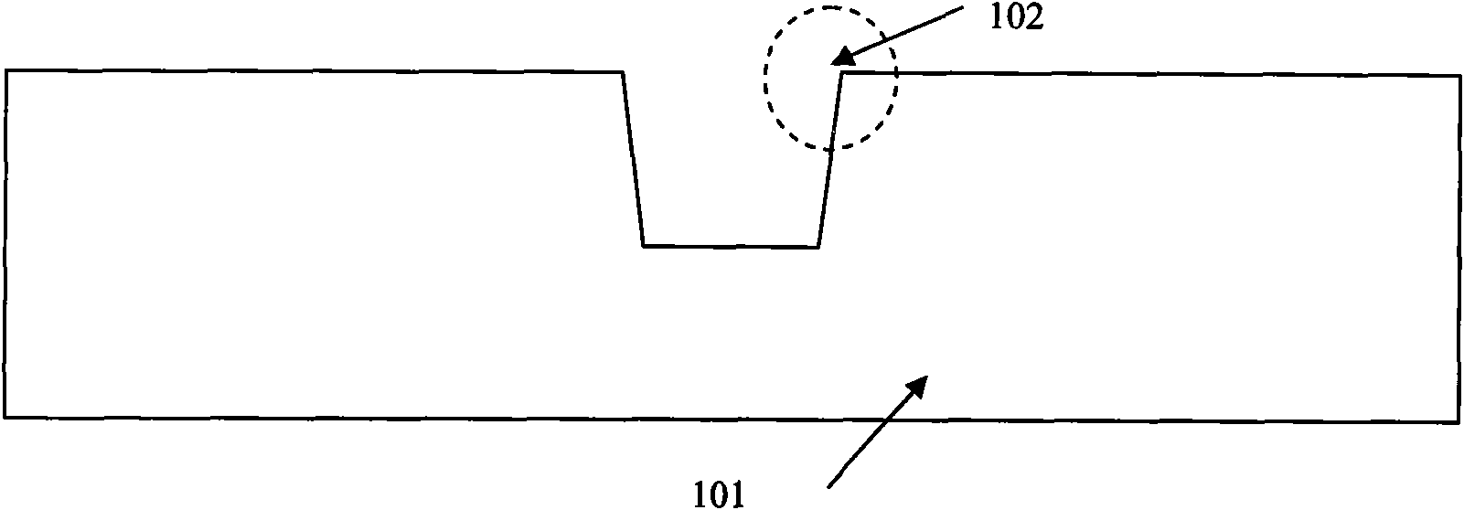
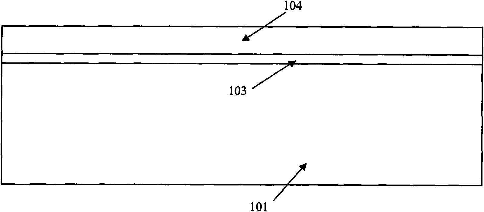
[0050] By analyzing the mechanism of the CMP process, it can help to understand the reasons for the formation of microcracks at the corners of the STI.

[0051] by image 3The silicon wafer shown is an example, in the CMP process, the silicon nitride layer 104 of the uppermost layer of the silicon wafer will be subjected to a downward pressure perpendicular to the plane where the silicon nitride layer 104 is located; in addition, due to the mutual movement of the silicon wafer and the polishing pad , the silicon nitride layer 104 is also subjected to a tangential force along the direction of the plane where the silicon nitride layer 104 is located. The corner 102 of the STI is where the silicon nitride layer 104 , the silicon oxide layer 103 , and the silicon substrate 101 meet. Under the action of the above pressure and tangential force, the internal stress concentration of the silicon wafer tends to occur. Under the action of internal stress, fine cracks will be generated i...


PUM


Abstract

The invention discloses a method for overcoming defects of a silicon chip with STI (Shallow Trench Isolation). A method for constructing STI on the silicon chip comprises the following steps of: depositing a pad oxides layer (103) and a silicon nitride layer (104) on a silicon substrate (101) of the silicon chip sequentially, covering the surface of the silicon chip by using photoresist, performing pattern transferring, and etching silicon nitride, pad oxide and the silicon chip by using the photoresist as a mask to construct an STI structure of which the bottom part is positioned in the silicon substrate. The method is characterized in that: After the silicon nitride layer (104) is deposited on the silicon chip and before the surface of the silicon chip is covered by the photoresist and pattern transferring is performed, the method comprises following step of: performing first annealing on the silicon chip to remove the internal stress of the silicon. The invention also discloses other methods for overcoming the defects of silicon chip with STI and methods for constructing the STI on the silicon chip. The technical scheme can effectively remove the internal stress of the silicon chip, thereby avoiding micro cracks in corners of the STI caused by internal stress and overcoming the defects of the surface of the silicon substrate.

Description

technical field [0001] The invention relates to the technical field of semiconductor integrated circuit processing, in particular to a method for suppressing defects of a silicon wafer with a shallow trench isolation (Shallow Trench Isolation, STI) structure and a method for constructing an STI on a silicon wafer. Background technique [0002] In the manufacturing process of semiconductor integrated circuits, it is often necessary to form a shallow trench isolation (Shallow Trench Isolation, STI) structure on a silicon wafer by etching. Such as figure 1 As shown, the silicon substrate 101 is composed of single crystal silicon, and the single crystal silicon is also called an active area (Active Area, AA). The concave portion in the center of the upper surface of the silicon substrate 101 is a shallow trench isolation trench formed by etching. Corners 102 are formed between the two sidewalls of the shallow trench isolation trench and the silicon substrate 101, namely figur...

Claims


Application Information

Patent Timeline
IPC IPC(8): H01L21/76H01L21/324
Inventor 潘继岗彭澎
Owner SEMICON MFG INT (SHANGHAI) CORP
Why Eureka
Try Eureka