Method for manufacturing gallium nitride-based light-emitting diode with current barrier layer

A technology for light-emitting diodes and current blocking layers, applied in circuits, electrical components, semiconductor devices, etc., can solve problems such as inability to use dry etching technology, surface passivation of p-type gallium nitride-based epitaxial layers, and damage to epitaxial layers. Achieve the effect of avoiding damage and passivation problems

Active Publication Date: 2011-02-09
XIAMEN SANAN OPTOELECTRONICS TECH CO LTD
View PDF2 Cites 26 Cited by
  • Summary
  • Abstract
  • Description
  • Claims
  • Application Information

AI Technical Summary

Problems solved by technology

The gallium nitride-based epitaxial layer is generally etched by dry method, but dry etching will cause damage to the epitaxial layer and form donor-like doping, which will cause surface passivation of the p-t...

Method used


Image

  • Method for manufacturing gallium nitride-based light-emitting diode with current barrier layer
  • Method for manufacturing gallium nitride-based light-emitting diode with current barrier layer
  • Method for manufacturing gallium nitride-based light-emitting diode with current barrier layer

Examples


Embodiment Construction

[0028] The present invention will be further described below in conjunction with the accompanying drawings and embodiments.

[0029] A method for manufacturing a GaN-based light-emitting diode with a current blocking layer, the manufacturing steps comprising:

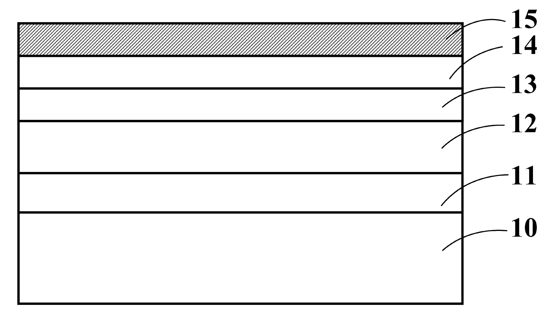
[0030] Such as figure 1 As shown, a buffer layer 11, an n-GaN layer 12, an MQW multiple quantum well 13, a p-GaN layer 14 and a u-GaN layer 15 are epitaxially grown on a sapphire substrate 10 in sequence to form a nitrogen GaN-based light-emitting epitaxial layer.

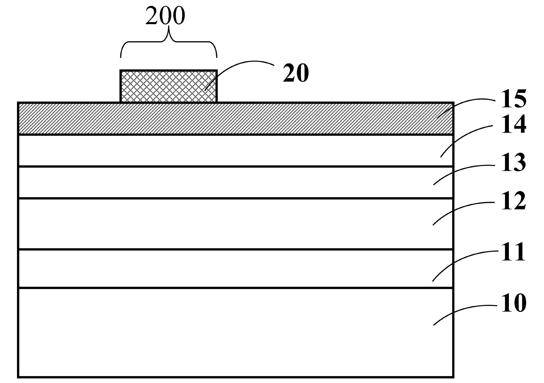
[0031] Such as figure 2 As shown, a Ti / Au mask layer 20 is vapor-deposited on the u-GaN layer 15 by electron beam evaporation method, with a thickness of 50 / 100nm, and a current blocking region 200 with a diameter of 110 microns is defined by photolithography. The Ti / Au mask layer 20 outside the current blocking region 200 is removed by etching.

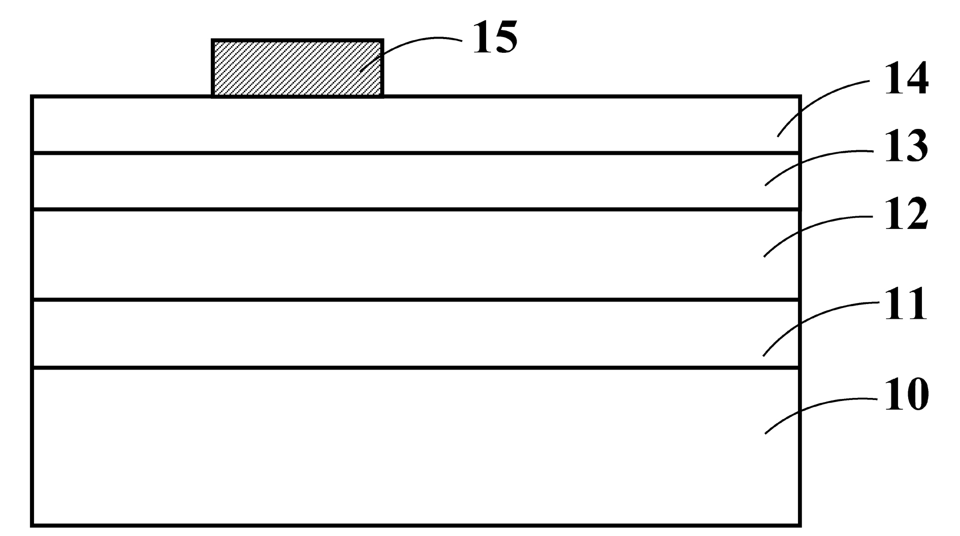
[0032] Such as image 3 As shown, the u-GaN layer 15 outside the current blocking region 200 is rem...


PUM


Abstract

The invention discloses a method for manufacturing a gallium nitride-based light-emitting diode with a current barrier layer. The method comprises the following steps of: constituting a gallium nitride-based luminous epitaxial layer by using an n-type gallium nitride-based epitaxial layer, an active layer, a p-type gallium nitride-based epitaxial layer and an undoped gallium nitride-based epitaxial layer from top to bottom in turn on a sapphire substrate; defining a current blocking area on the gallium nitride-based luminous epitaxial layer and coating a metal layer serving as a mask on the undoped gallium nitride-based epitaxial layer of the current blocking area so as to cover the entire current blocking area; removing the undoped gallium nitride-based epitaxial layer outside the current blocking area by electrochemical etching; removing the metal layer serving as the mask; manufacturing a transparent conductive layer on the p-type gallium nitride-based epitaxial layer and the undoped gallium nitride-based epitaxial layer; and manufacturing a p electrode on the transparent conductive layer in the current blocking area. The current barrier layer is defined selectively by the electrochemical etching, so that the problems of damage and passivation caused by dry etching are solved and an undoped epitaxial layer-based gallium nitride-based light-emitting diode with current blocking effect is obtained.

Description

technical field [0001] The invention relates to a method for manufacturing a light-emitting diode chip, in particular to a method for manufacturing a gallium nitride-based light-emitting diode with a current blocking layer. Background technique [0002] In traditional light-emitting diodes, metal electrodes are generally placed on the top of the chip. On the one hand, it is for better expansion of the current, and on the other hand, it must also provide pads for bonding wires; but the existence of metal electrodes will cause the active layer to emit light. The light of the LED is blocked, and the reflectivity of most metal electrodes is not high, so the light extraction efficiency of the LED will be reduced. In order to prevent the light emitted by the active layer from being blocked or absorbed by the metal electrode, it is necessary to suppress or reduce the carrier transport and recombination light emission in the active layer directly below the metal electrode. One of t...

Claims


Application Information

Patent Timeline
IPC IPC(8): H01L33/00
Inventor 潘群峰吴志强黄少华
Owner XIAMEN SANAN OPTOELECTRONICS TECH CO LTD
Why Eureka
Try Eureka