Semiconductor structure for increasing integration density of high-voltage integrated circuit device and manufacturing method

A high-voltage integrated circuit, integration density technology, applied in semiconductor/solid-state device manufacturing, semiconductor devices, circuits, etc., can solve problems such as poor clamping, reduce processing time, improve the controllability of epitaxy quality, and reduce processing temperature. Effect

Active Publication Date: 2011-02-16
NO 24 RES INST OF CETC
View PDF3 Cites 6 Cited by
  • Summary
  • Abstract
  • Description
  • Claims
  • Application Information

AI Technical Summary

Problems solved by technology

[0007] Aiming at the problems of increased circuit area in the above-mentioned high-voltage integrated circuit and high steps, high electric field, high stress and poor clamping of the deep trench isolation sidewall dielectric layer, the present invention provides a semiconductor structure that increases the integration density of high-voltage integrated circuit devices and manufacturing method

Method used


Image

  • Semiconductor structure for increasing integration density of high-voltage integrated circuit device and manufacturing method
  • Semiconductor structure for increasing integration density of high-voltage integrated circuit device and manufacturing method
  • Semiconductor structure for increasing integration density of high-voltage integrated circuit device and manufacturing method

Examples


Embodiment Construction

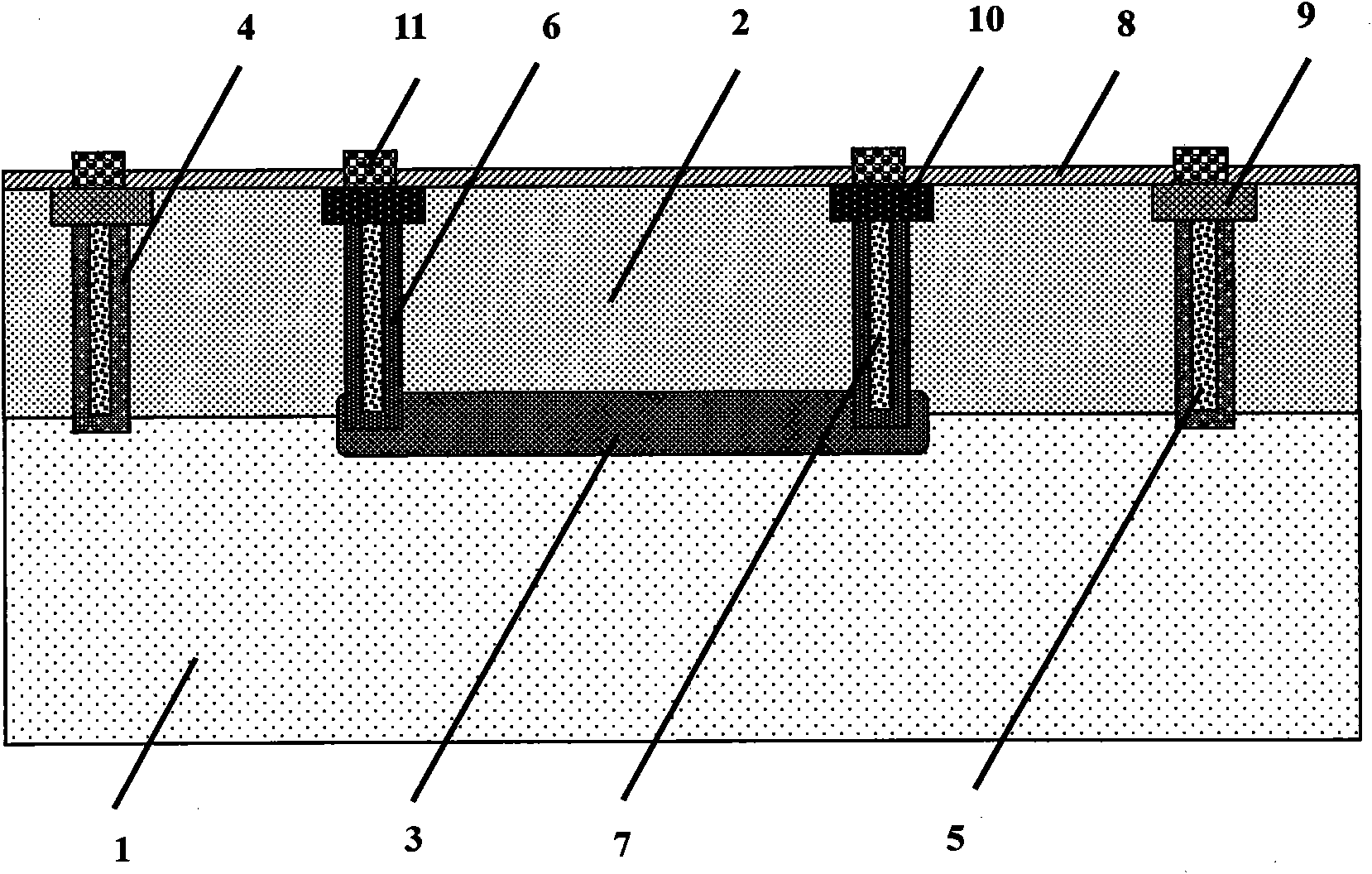
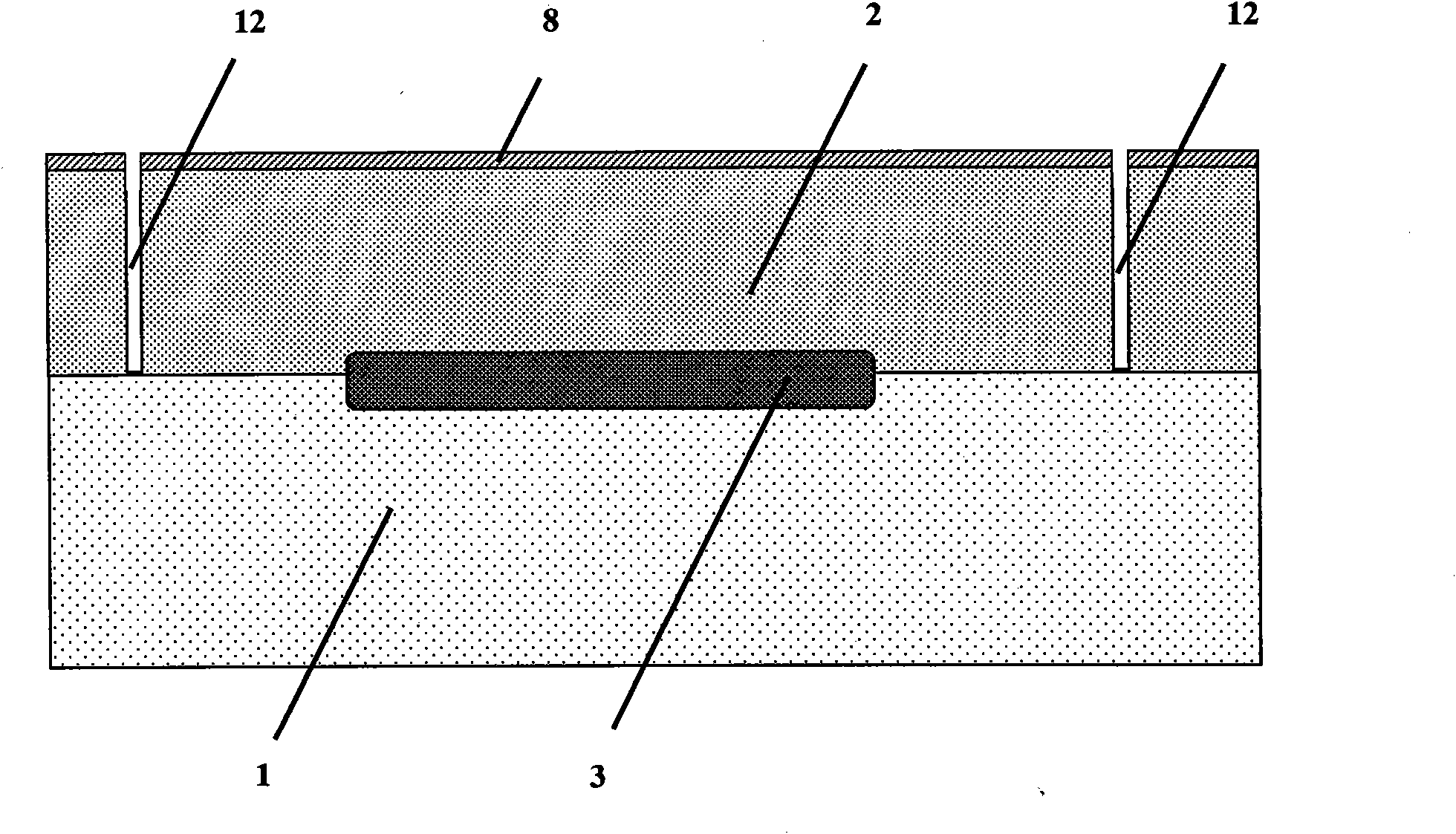
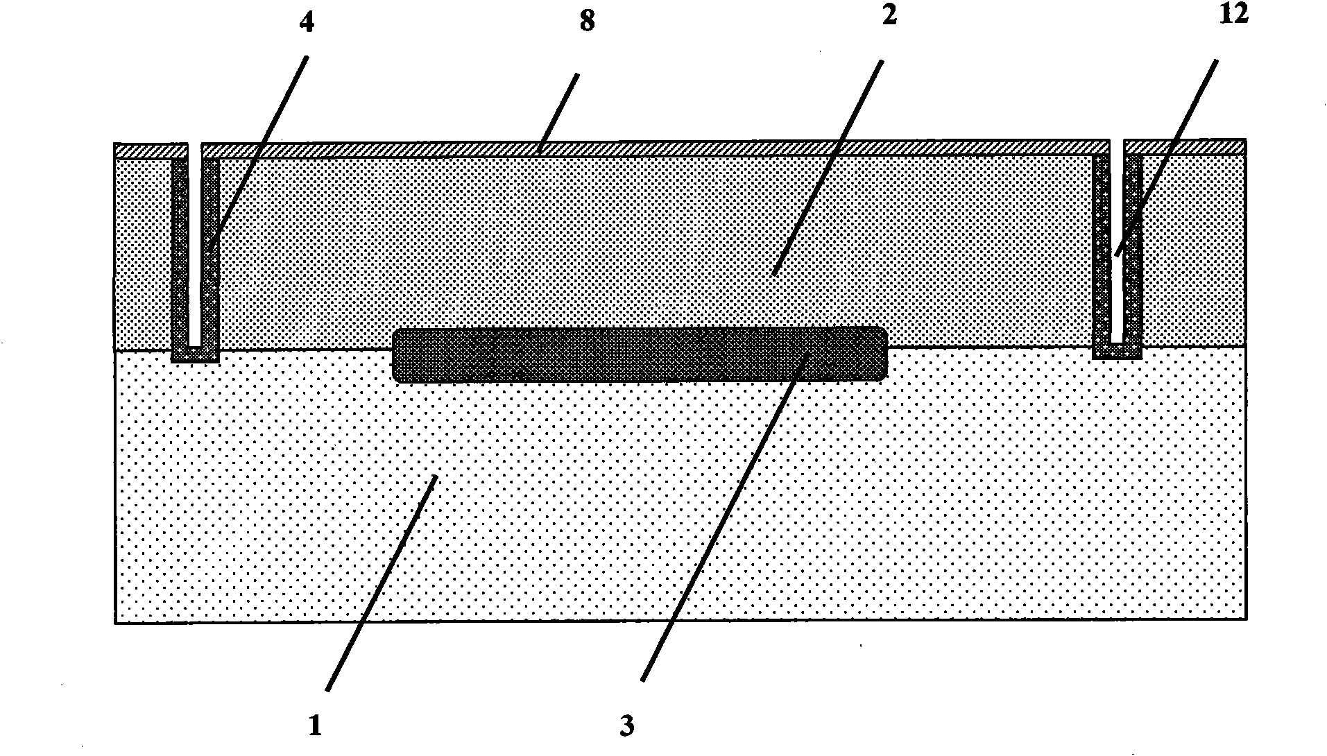
[0030] The specific implementation of the present invention is not limited to the semiconductor device described below, but also can increase the integration density of high-voltage integrated circuit devices by adopting various similar methods well known in the industry that can meet the requirements of this manufacturing method according to the core and design spirit of this method the goal of.

[0031] Taking a 40V high-voltage bipolar integrated circuit as an example, the specific implementation steps of a semiconductor structure and a manufacturing method for increasing the integration density of high-voltage integrated circuit devices of the present invention are as follows:

[0032] 1. On a 7-20Ω.cm, P-type semiconductor substrate 1, a 600-650nm oxide layer is formed by oxidation or CVD low deposition methods commonly used in the industry, and a 30-50nm oxide layer is formed by photolithography and thin oxygen, and then 150KeV, (2~8)×10 15 cm -2 , As ion implantation...


PUM


Abstract

The invention relates to a semiconductor structure for increasing integration density of a high-voltage integrated circuit device and a manufacturing method. Aiming at the problems of large occupation area of PN junction isolation and penetration diffusion adopted in a high-voltage integrated circuit and high step, high electric field, high stress and poor clamping hidden trouble of conventional deep slot isolation, a deep slot diffusion isolation and deep slot penetration diffusion structure is adopted to realize improvement on the integration density of the high-voltage device and promotion on the performance of the device. The method can reduce over 35 percent of high-voltage integrated circuit area at most, improve the integration density of the high-voltage integrated circuit, thin the thickness of an epitaxial layer compared with the common penetration structure, simplify the process design of the high-voltage integrated circuit device structure and effectively solve the high step, high electric field, high stress and poor clamping hidden trouble of the conventional deep slot isolation structure. The method is applied in the fields of structure design and manufacture of high-voltage semiconductor devices and integrated circuits.

Description

technical field [0001] The invention relates to a semiconductor structure of a high-voltage-resistant semiconductor integrated circuit, in particular to a semiconductor structure and a manufacturing method for increasing the integration density of a high-voltage integrated circuit device, which is suitable for the structural design and manufacturing fields of a high-voltage semiconductor device and an integrated circuit. Background technique [0002] In the structure and manufacture of high-voltage semiconductor devices and integrated circuits, especially those that require isolation between devices within the semiconductor and low-resistance connections deep inside, PN junction isolation and buried diffusion layers ( hereinafter referred to as the buried layer) plus the same type of penetration diffusion layer (hereinafter referred to as penetration), combined with silicon wafer epitaxy and other methods to obtain an appropriate structure to meet the needs of specific integr...

Claims


Application Information

Patent Timeline
Patent Type & Authority Applications(China)
IPC IPC(8): H01L21/761H01L21/22H01L21/306H01L29/06
Inventor 谭开洲张静张正璠
Owner NO 24 RES INST OF CETC
Why Eureka
Try Eureka