Structure of ultra-thin crystal-silicon solar battery pack and packaging method thereof
A technology for solar cells and solar cells, applied in electrical components, circuits, photovoltaic power generation, etc., can solve the problems of increased component cost, reduced application occasions, increased component weight, etc., to achieve the effect of reduced production cost and great application prospects.
- Summary
- Abstract
- Description
- Claims
- Application Information
AI Technical Summary
Problems solved by technology
Method used
Image
Examples
Embodiment 1
[0036] Use the following steps for ultra-thin crystalline silicon solar cell module packaging:
[0037] Sorting-Single welding and string welding of solar cells-Laying ribs on the back panel-Laying EVA film on the back plate-Laminated solar cells-Laying EVA film-Laying surface cover plate-Lamination-Cutting edge-Framing- test.
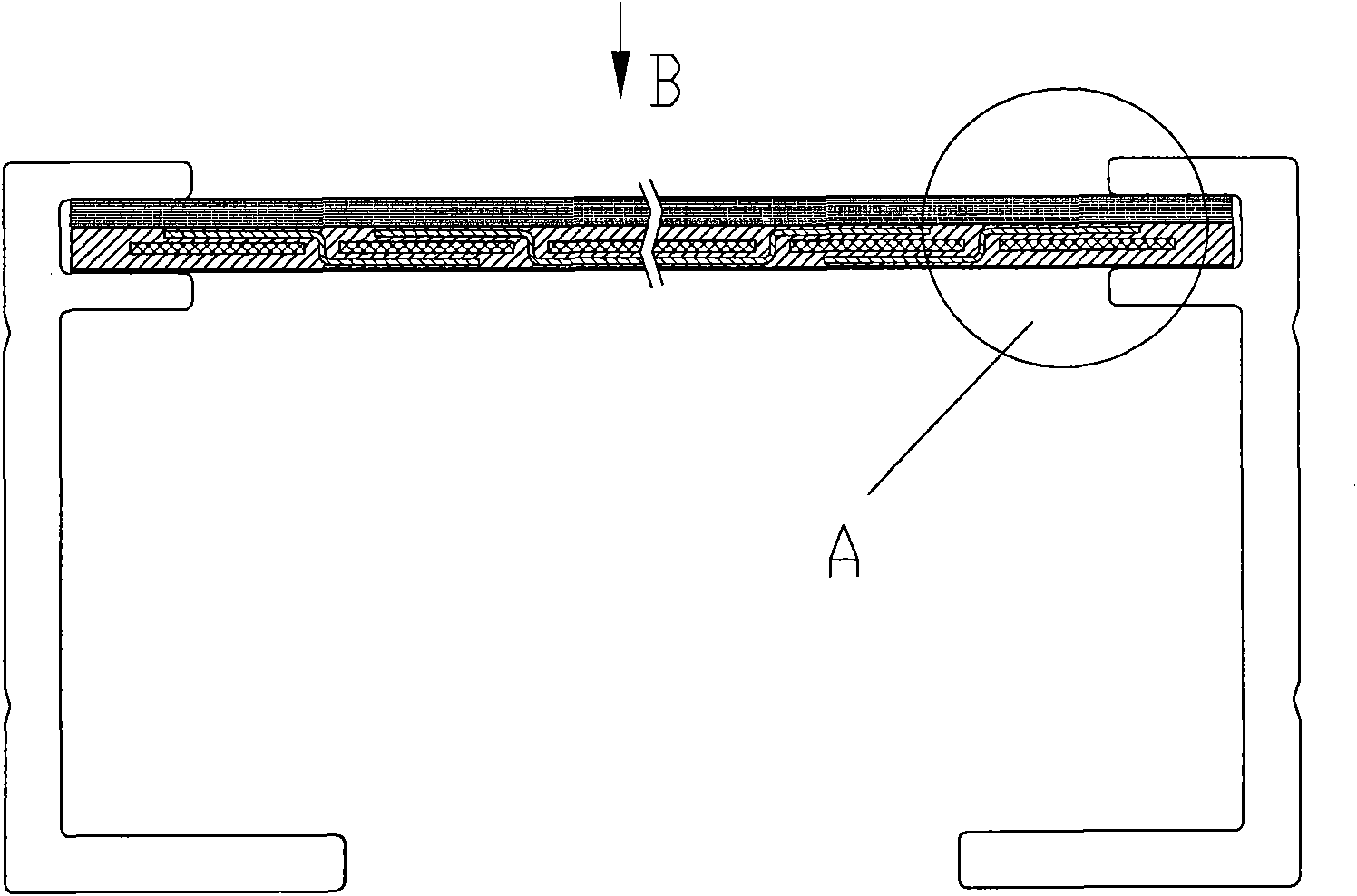
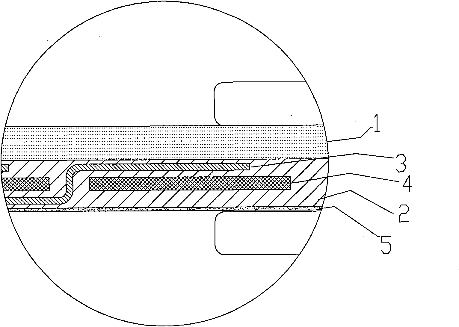
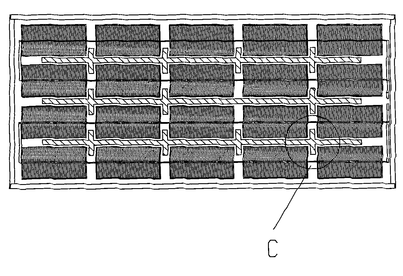
[0038] and get as figure 1 , 2 , The ultra-thin crystalline silicon solar cell module of structure shown in 3, 4, it comprises back plate 5, is laid with EVA adhesive film 4 on the back plate 5, is arranged with solar cells 2 at intervals in EVA adhesive film 4, solar cell The sheets 2 are connected to each other by photovoltaic ribbons 3, the surface cover plate 1 is laid on the EVA film 4, and the reinforcing ribs 6 are provided between the back plate 5 and the EVA film 4 laid on the back plate 5, and the reinforcing ribs 6 is arranged in the interval area between the solar cells 2 , that is, the reinforcing ribs 6 will not cover the solar cells 2...
Embodiment 2
[0040] Use the following steps for ultra-thin crystalline silicon solar cell module packaging:
[0041] Sorting - single welding and string welding of solar cells - laying EVA film on the back plate - laying ribs on the EVA film - stacking solar cells - laying EVA film - laying surface cover plate - lamination - trimming - framing -test.
[0042] and get as figure 1 , 2 , The ultra-thin crystalline silicon solar cell module of structure shown in 3, 4, it comprises back plate 5, is laid with EVA adhesive film 4 on the back plate 5, is arranged with solar cells 2 at intervals in EVA adhesive film 4, solar cell The sheets 2 are connected to each other by photovoltaic ribbons 3, the surface cover plate 1 is laid on the EVA film 4, and the reinforcing ribs 6 are laid inside the EVA film 4 laid on the back plate 5, and the reinforcing bars 6 are arranged on the solar panel. In the interval area between the solar cells 2 , that is, the ribs 6 will not cover the solar cells 2 .
Embodiment 3
[0044] Use the following steps for ultra-thin crystalline silicon solar cell module packaging:
[0045] Sorting - single welding and string welding of solar cells - laying EVA film on the back plate - stacking solar cells - laying reinforcing ribs on the EVA film - laying EVA film - laying surface cover plate - lamination - trimming - framing -test.
[0046] and get as figure 1 , 2, The ultra-thin crystalline silicon solar cell module of structure shown in 3, 4, it comprises back plate 5, is laid with EVA adhesive film 4 on the back plate 5, is arranged with solar cells 2 at intervals in EVA adhesive film 4, solar cell The sheets 2 are connected to each other by photovoltaic ribbons 3, the surface cover plate 1 is laid on the EVA film 4, and the reinforcing ribs 6 are laid inside the EVA film 4 laid on the back plate 5, and the reinforcing bars 6 are arranged on the solar panel. In the interval area between the solar cells 2 , that is, the ribs 6 will not cover the solar ce...
PUM
 Abstract
Description
Claims
Application Information


