Controllable self-clamping SensorFET composite lateral power device

A technology of lateral power devices and power converters, which is applied in the electronic field and can solve problems such as device temperature rise and inability to discharge avalanche energy

Inactive Publication Date: 2011-11-16
UNIV OF ELECTRONICS SCI & TECH OF CHINA
View PDF1 Cites 0 Cited by
  • Summary
  • Abstract
  • Description
  • Claims
  • Application Information

AI Technical Summary

Problems solved by technology

Since the device width of the SensorFET is usually much smaller than the width of the main switching device, the above-mentioned high-voltage SensorFET device faces the problem that it cannot effectively discharge the avalanche energy when the main switching device is turned off. At this time, the high-voltage SensorFET is placed in a high-voltage or / and high current conditions, the device temperature will rise rapidly

Method used


Image

  • Controllable self-clamping SensorFET composite lateral power device
  • Controllable self-clamping SensorFET composite lateral power device
  • Controllable self-clamping SensorFET composite lateral power device

Examples


specific Embodiment approach 1

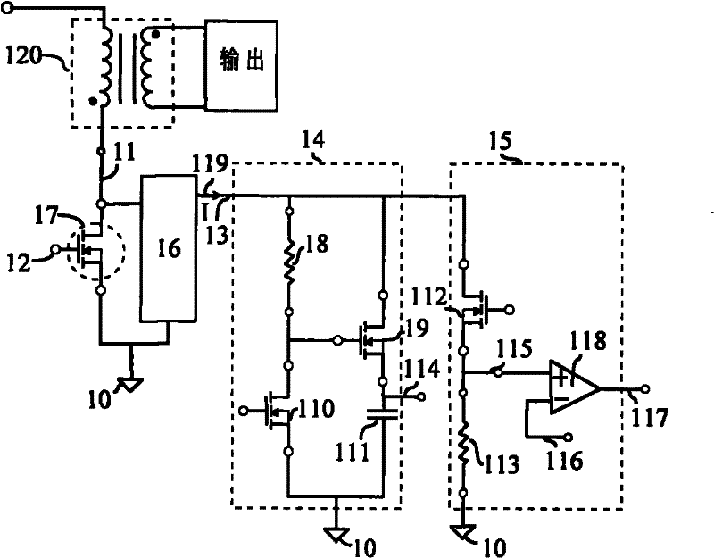
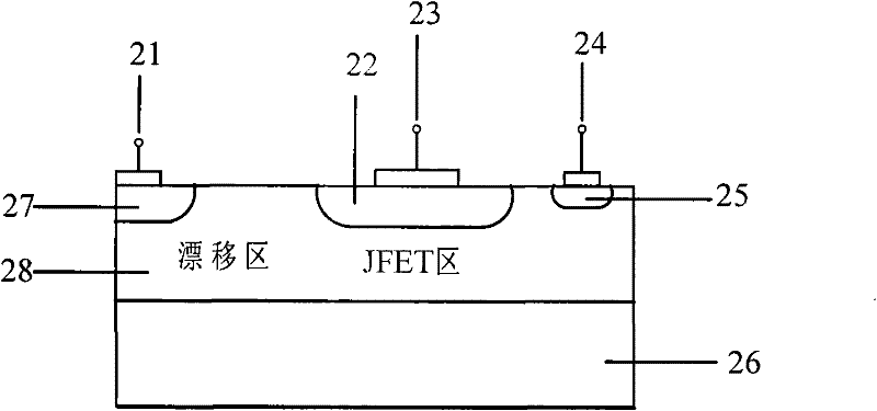
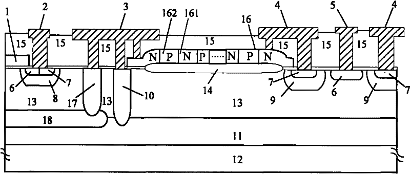
[0024] A controllable self-clamping SensorFET composite lateral power device, such as image 3 As shown, it includes a main switching tube of a power converter and a SensorFET device; the main switching tube and the SensorFET device of the power converter are integrated on the same P-type substrate 11 .

[0025] The SensorFET device includes: a first P-type layer 9, N - A Double-RESURF structure composed of the drift region 10 and the P-type substrate 11, wherein the first P-type layer 9 is located in the N - In the drift region 10; a N connected by the metal cathode electrode 1 + District 6, N - The N connected to the drift region 10 and the metal anode 3 + The charging and current detection channel formed by region 6, in which the metal cathode electrode 1 is connected to the N + N + Region 6 is respectively located on the N sides of the first P-type layer 9 - In the drift region 10; a clamping diode string formed alternately by N-type polysilicon 131 and P-type polysi...

specific Embodiment approach 2

[0028] A controllable self-clamping SensorFET composite lateral power device, such as Figure 4 As shown, it includes a main switching tube of a power converter and a SensorFET device; the main switching tube and the SensorFET device of the power converter are integrated on the same P-type substrate 11 .

[0029] The SensorFET device includes: a first P-type layer 9, N - A Double-RESURF structure composed of the drift region 10 and the P-type substrate 11, wherein the first P-type layer 9 is located in the N - In the drift region 10; a N connected by the metal cathode electrode 1 + District 6, N - The N connected to the drift region 10 and the metal anode 3 + The charging and current detection channel formed by region 6, in which the metal cathode electrode 1 is connected to the N + N + Region 6 is respectively located on the N sides of the first P-type layer 9 - In the drift region 10; a clamping diode string formed alternately by N-type polysilicon 131 and P-type polys...


PUM


Abstract

The invention discloses a controllable self-clamping SensorFET composite lateral power device and belongs to the fields of semiconductor power device technology and power integrated circuit technology. A main switching tube of a power inverter and a SensorFET device are integrated on the same P-type substrate and adopt a shared anode structure, wherein a clamping diode string is arranged between a control electrode of the SensorFET device and the shared anode; and the main switching tube of the power inverter can be a lateral metal oxide semiconductor (MOS) composite device or a conventional MOS device. The provided controllable self-clamping SensorFET composite lateral power device can provide stable charging current for an interior circuit and effectively release avalanche energy, so a transient safety operation area of the SensorFET device is expanded. Meanwhile, due to the connection of a clamping tube and a control grid area, the energy release and clamping time are controlled soas to expand the application of an intelligent power integrated circuit (IC) under a high-avalanche energy environment, such as the field of ignition.

Description

technical field [0001] The invention belongs to the field of electronic technology, and relates to semiconductor power device technology and power integrated circuit technology. Background technique [0002] The power integrated circuit is the interface circuit between the control circuit and the power load. Its simplest circuit includes a level shifter and a drive circuit. Its function is to convert the logic signal level output by the microprocessor into a drive signal sufficient to drive the load. level. Power integrated circuits appeared in the late 1970s. Due to single-chip integration, power integrated circuits reduce the number of components, interconnections and solder joints in the system, which not only improves the reliability and stability of the system, but also reduces the number of components in the system. power consumption, size, weight and cost. Be able to self-manage the working state, respond to emergencies and take corresponding countermeasures (called...

Claims


Application Information

Patent Timeline
Patent Type & Authority Patents(China)
IPC IPC(8): H01L27/02H01L29/06H01L29/417
CPCH01L29/87H01L29/0634H01L29/402
Inventor 李泽宏邓光平钱振华胡涛洪辛张波
Owner UNIV OF ELECTRONICS SCI & TECH OF CHINA
Why Eureka
Try Eureka