Four-junction solar photovoltaic cell chip for compound semiconductor

A photovoltaic cell and semiconductor technology, which is applied in the field of four-junction compound semiconductor solar photovoltaic cell chip structure, can solve the problems such as the failure to obtain effective absorption and utilization of energy with absorption efficiency, and the low photoelectric conversion efficiency of solar cell chips. The effect that the current cannot be fully absorbed, the photoelectric conversion efficiency is improved, and the absorption spectrum range is expanded

Active Publication Date: 2011-02-23
ZHONGSHAN DEHUA CHIP TECH CO LTD
View PDF5 Cites 4 Cited by
  • Summary
  • Abstract
  • Description
  • Claims
  • Application Information

AI Technical Summary

Problems solved by technology

[0003] However, the relatively low photoelectric conversion efficiency of existing solar cell chips restricts its further wide application in practical work and life. This is because the solar radiation energy flow is asymmetrically distributed in the peak wavelength of about 500nm, from the ultraviolet 200nm band to In the wide spectral range of the far-infrared 2600nm band, especially in my country's Tibet, Xinjiang and other high

Method used


Image

  • Four-junction solar photovoltaic cell chip for compound semiconductor
  • Four-junction solar photovoltaic cell chip for compound semiconductor

Examples


Embodiment Construction

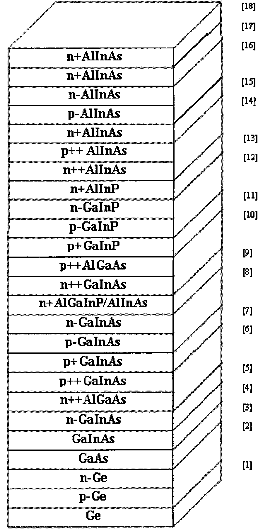
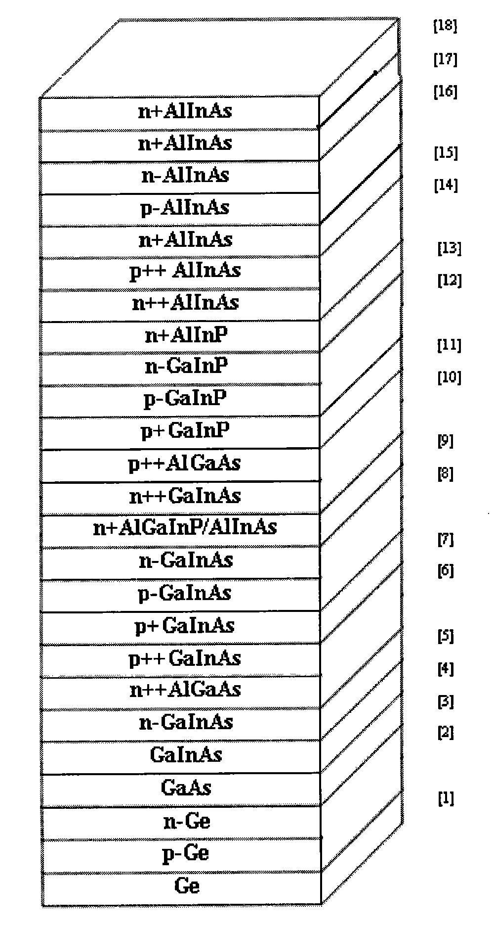
[0011] In order to further illustrate the structure and features of the present invention, the present invention will be further described below in conjunction with the embodiments and accompanying drawings. Such as figure 1 As shown, the four-junction compound semiconductor solar photovoltaic cell chip adopts the metal organic chemical vapor deposition (MOCVD) method, and the bottom cell chip (p-Ge, n-Ge) 2 is sequentially grown on the germanium (Ge) single wafer 1 as the substrate, forming Core layer (GaAs) 3, buffer layer (GaInAs) 4, barrier layer (n-GaInAs) 5, tunnel junction (n++AlGaAs, p++GaInAs) 6, barrier layer (p+GaInAs) 7, the Two-junction cell (p-GaInAs, n-GaInAs) 8, window layer (n+AlGaInP / AlInAs) 9, second tunnel junction (n++GaInAs, p++AlGaAs) 10, second barrier layer (p+ GaInP) 11, the third junction cell (p-GaInP, n-GaInP) 12, the second window layer (n+AlInP) 13, the third tunnel junction (n++AlInAs, p++AlInAs) 14, the third potential Barrier layer (n+AlInAs...


PUM


Abstract

The invention discloses a four-junction solar photovoltaic cell chip for a compound semiconductor and belongs to the technical field of semiconductor optic electronics. The key point is that: a top cell made of an AlInAs material with high forbidden bandwidth is arranged on the conventional multi-junction solar cell chip material system. The AlInAs material is used as the top cell to be attached to the conventional multi-junction solar cell chip material system, so the range of the absorption spectrum of the solar cell chip can be widened, the problem that the solar cell chip cannot fully absorb massive energy flow of solar radiation distributed at an ultraviolet band is effectively solved, and the photoelectric conversion efficiency of the multi-junction solar cell chip is improved.

Description

technical field [0001] The invention relates to a four-junction compound semiconductor solar photovoltaic cell chip structure, which belongs to the technical field of semiconductor optoelectronics. Background technique [0002] When non-renewable energy sources such as electricity, coal, and oil are in urgent need, and energy issues are increasingly becoming a bottleneck restricting the development of the international society and economy, solar energy has attracted special attention due to its inexhaustible, inexhaustible and zero-pollution characteristics. More and more countries have begun to implement the "Sunshine Plan" to develop solar energy resources and seek new impetus for economic development. In the long run, with the improvement of solar cell chip manufacturing technology and the invention of new photoelectric conversion devices, combined with the protection of the environment and the huge demand for renewable and clean energy in various countries, solar cell ch...

Claims


Application Information

Patent Timeline
IPC IPC(8): H01L31/04H01L31/0352H01L31/078
CPCY02E10/50
Inventor 王智勇李建军尧舜
Owner ZHONGSHAN DEHUA CHIP TECH CO LTD
Why Eureka
Try Eureka