

Surface processing method of Auger electron spectrometer detecting sample
A technology of surface treatment and Auger electron, which is applied in the field of surface treatment of samples detected by Auger electron spectrometer, can solve the problems of platinum or silver signal weakening, covering, interference, etc., to reduce charging effect and avoid cost , improve the effect of signal-to-noise ratio
- Summary
- Abstract
- Description
- Claims
- Application Information
AI Technical Summary
Problems solved by technology
Method used
Image

Examples
Embodiment Construction
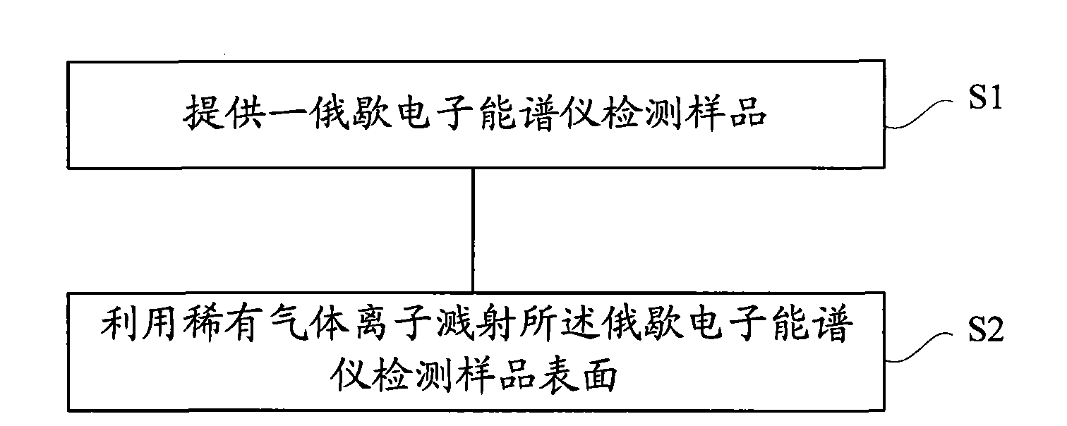
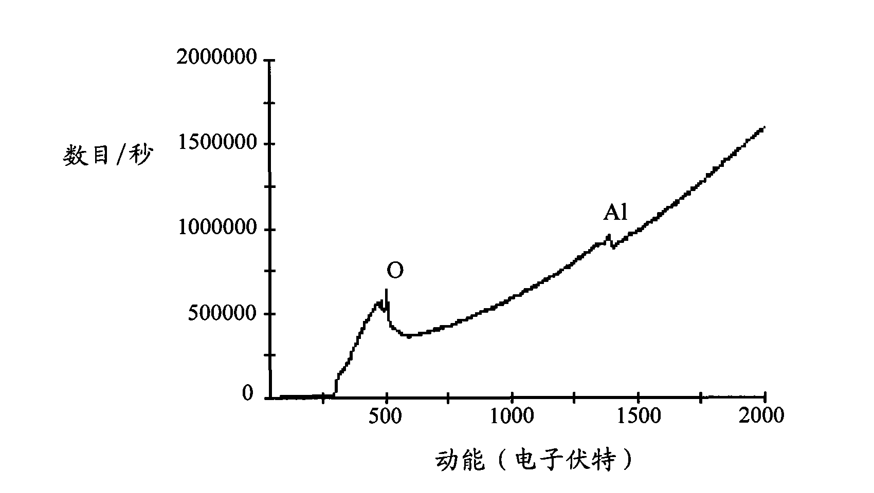
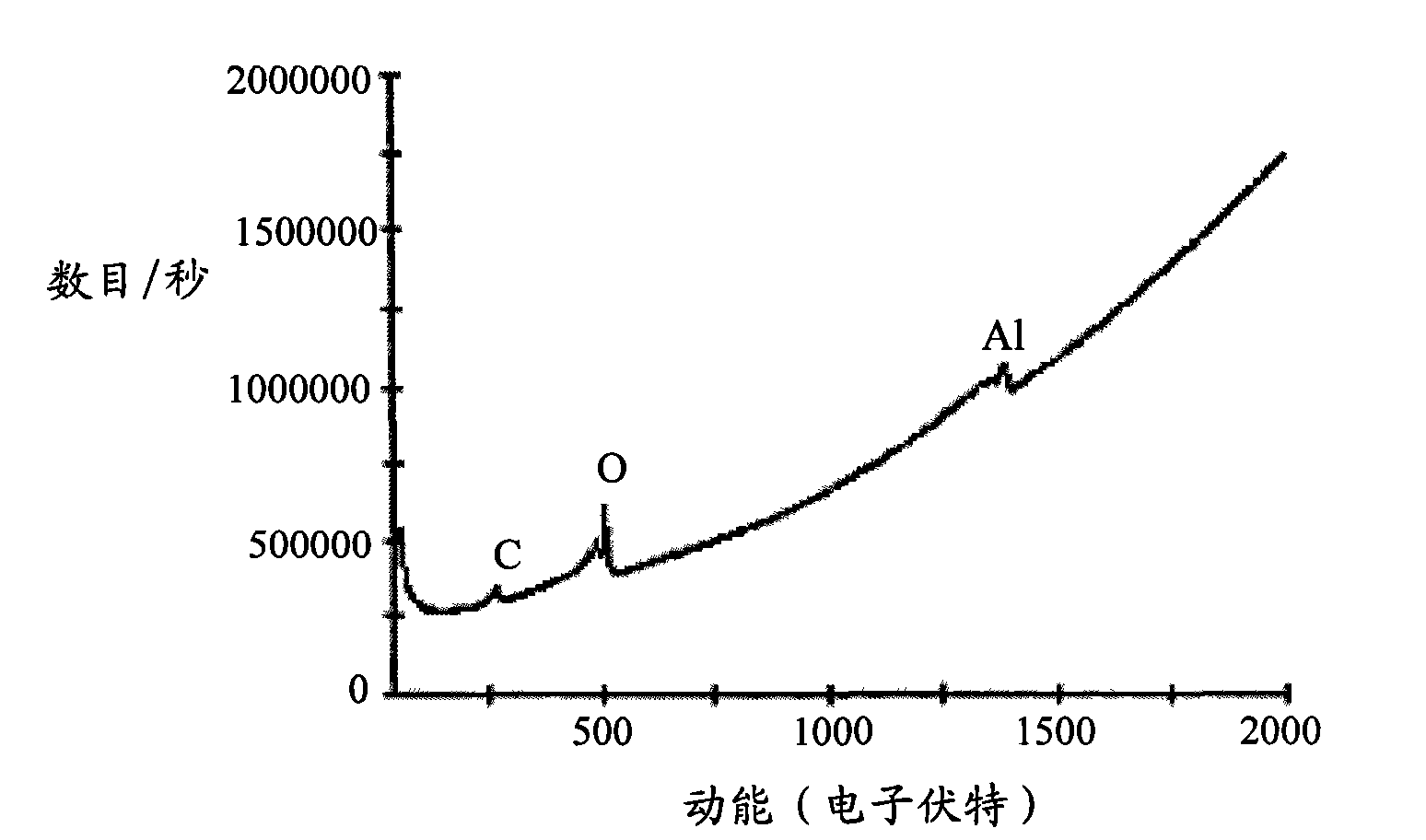
[0027] The invention will now be described in more detail with reference to the accompanying drawings, in which preferred embodiments of the invention are shown, it being understood that those skilled in the art may modify the invention described herein and still achieve the advantageous effects of the invention. Therefore, the following description should be understood as the broad knowledge of those skilled in the art, but not as a limitation of the present invention.
[0028] In the interest of clarity, not all features of an actual implementation are described. In the following description, well-known functions and constructions are not described in detail since they would obscure the invention with unnecessary detail. It should be appreciated that in the development of any actual embodiment, numerous implementation details must be worked out to achieve the developer's specific goals, such as changing from one embodiment to another in accordance with system-related or busi...
PUM
 Abstract
Description
Claims
Application Information