


Quick Research
Generate reliable direction feasibility study reports for your R&D in just a few steps.

Technical Q&A
Discover and master advanced knowledge NOW. Basics, ideas, possibilities, all at once.

Find Solutions
As an expert in R&D theories, this can generate solutions to your technical problems instantly.

Evaluate Feasibility
Analyze your overall solution with one click, know your potential R&D risks in advance.

Monitor Landscape
Get weekly tech updates, stay abreast of the latest tech innovations and key insights.
Method for forming bumps
A technology of bumps and metal layers under bumps, used in electrical components, semiconductor/solid-state device manufacturing, circuits, etc. problems, to avoid short circuits and open circuits, keep the size consistent, and eliminate voids
- Summary
- Abstract
- Description
- Claims
- Application Information
AI Technical Summary
Problems solved by technology
Method used
Image

Examples
Embodiment Construction
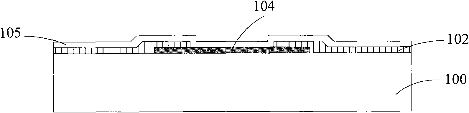
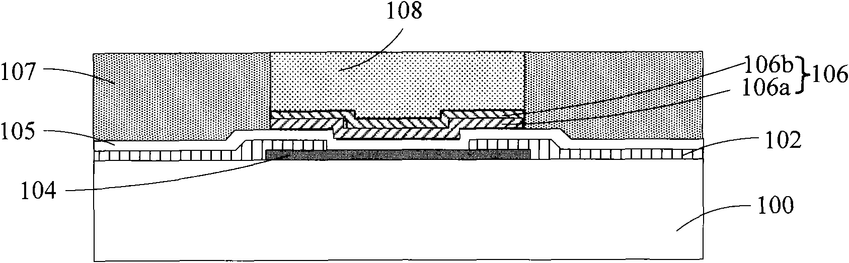
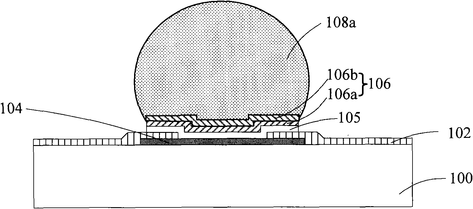
[0026] In an embodiment of the present invention, a semiconductor substrate with defects is placed in an electrolytic cell and a current is applied to react to remove the defects, and a solution containing hydrogen ions or hydroxide ions is injected into the electrolytic cell. Utilize the defects in the oxide-containing metal layer to interact with hydroxide ions or hydrogen ions to form metal molecules, and then provide the electrons required for the reaction by applying an external potential, so that the hydrogen ions or hydroxide ions produce corresponding potential effects. Defects are removed, thereby eliminating voids generated in subsequent bumps, keeping the size of all bumps consistent, avoiding the occurrence of short circuits and open circuits, and improving the quality of packaging.
[0027] The present invention provides the concrete flow process of making bump as Figure 5 As shown, step S11 is performed to provide a semiconductor substrate, on which a metal pad ...
PUM
 Abstract
Description
Claims
Application Information
 - R&D Engineer
- R&D Manager
- IP Professional
- Industry Leading Data Capabilities
- Powerful AI technology
- Patent DNA Extraction
Browse by: Latest US Patents, China's latest patents, Technical Efficacy Thesaurus, Application Domain, Technology Topic, Popular Technical Reports.
© 2024 PatSnap. All rights reserved.Legal|Privacy policy|Modern Slavery Act Transparency Statement|Sitemap|About US| Contact US: help@patsnap.com