
Method for implementing flip-chip soldering of solder during soldering in groove

An undercut and solder technology, applied in the field of microelectronic packaging, can solve problems such as hidden dangers in reliability, and achieve the effect of preventing short-circuiting

Active Publication Date: 2011-03-30
SHANGHAI IND U TECH RES INST
View PDF4 Cites 6 Cited by
  • Summary
  • Abstract
  • Description
  • Claims
  • Application Information

AI Technical Summary

Problems solved by technology

"Semi-additive process" can reduce the spacing between pads, but the disadvantage is that a seed layer must be used, and the reliability of the contact between the seed layer and the surrounding medium may have hidden dangers

Method used


Image

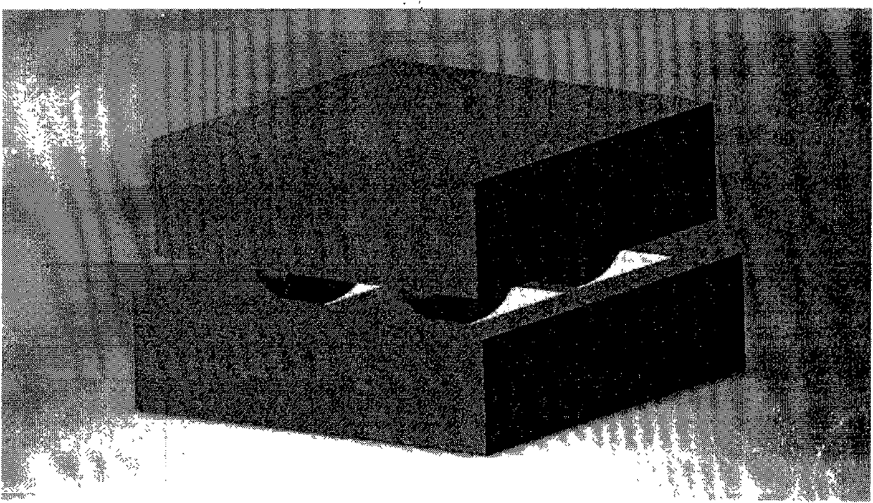
  • Method for implementing flip-chip soldering of solder during soldering in groove
  • Method for implementing flip-chip soldering of solder during soldering in groove
  • Method for implementing flip-chip soldering of solder during soldering in groove

Examples


Embodiment 1

[0028] The process method of solder undercut welding provided by the invention, concrete steps are:

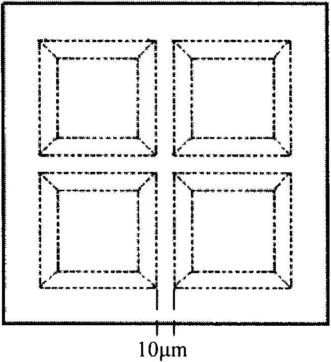
[0029] ①Use an N-type silicon wafer with a thickness of 400-600 μm as the upside-down welding substrate, and use a TMAH solution with a concentration of 25% on the substrate to perform wet etching to form a corrosion opening. The corrosion opening is in the shape of a chute, and the gap between adjacent chute The distance is 10 μm, the inclination angle of the side wall of the chute is 54.7°, the size of the corrosion opening is 64×64 μm, and the depth is 20 μm ( figure 2 );

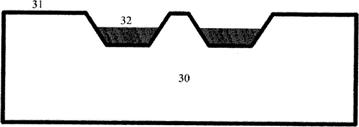
[0030] ② Using the full additive process, make copper pads in the chute ( image 3 )

[0031] a) firstly sputtering a TiW / Cu seed layer on the upper surface of the substrate after etching the opening and passivating in step ①;

[0032] b) glue spraying and photolithography, remove the photoresist at the bottom of the chute, and keep the photoresist on the sidewall of the chute and the periphery of th...


PUM

PropertyMeasurementUnit
Thicknessaaaaaaaaaa
Thicknessaaaaaaaaaa

Abstract

The invention relates to a process for implementing flip-chip soldering of solder during soldering in groove, characterized by comprising the steps of: (1) using a common silicon wafer as a flip-chip soldering substrate and forming an oblique groove on the substrate by TMAH wet method; (b) manufacturing copper pads in the oblique groove by full addition method without the preparation of a solder mask; and (c) achieving the alignment between tin bumps and the pads in the oblique groove by a flip-chip soldering machine, and inserting the bumps into the oblique groove and soldering the bumps with the pads. The process of the invention finally can realize the pad structure with the pad spacing of 74 microns and the pad width of 50 microns, superior to current relational parameters between pad area and pad spacing resulted from subtraction process and semi-addition process. Besides, the flip-chip soldering process has no need of manufacturing the solder mask structure, and the groove can limit the flowing of solder by means of the blocking effect of an etch bath in order to prevent short circuit between adjacent pads, which is caused by the flowing of solder in the process of reflux.

Description

technical field [0001] The invention relates to a process method for realizing upside-down welding by welding in grooves, and belongs to the field of microelectronic packaging. Background technique [0002] The goal of microelectronic packaging technology has always been to provide chips with simpler, cheaper, smaller size, and higher density packages. Flip-Chip Technology can directly realize the welding between the bump and the pad, and the process is simple; the interconnection structure formed after welding is small in size, which effectively reduces the parasitic loss. The upside-down welding process has standard regulations on the relationship between the area of ​​the pad and the spacing between the pads to ensure the strength and reliability of the package. [0003] There are generally two methods for the preparation of copper pads in the upside-down welding process. One is called "subtractive process", that is, a photolithography process is first performed on a co...

Claims


Application Information

Patent Timeline
IPC IPC(8): H01L21/60
CPCH01L2224/81
Inventor 曹毓涵罗乐徐高卫袁媛
Owner SHANGHAI IND U TECH RES INST
Learn More