DRAM (Dynamic Random Access Memory) structure with expansion groove and manufacturing method thereof

A trench and N-type technology, which is applied in the manufacture of semiconductor/solid-state devices, transistors, electrical components, etc., can solve the problems of high etching process requirements, affecting yield, complex process, etc., to overcome low leakage thin dielectric layer , Large capacitor plate area, simple process effect

Inactive Publication Date: 2012-07-04
SHANGHAI INST OF MICROSYSTEM & INFORMATION TECH CHINESE ACAD OF SCI
View PDF0 Cites 6 Cited by
  • Summary
  • Abstract
  • Description
  • Claims
  • Application Information

AI Technical Summary

Problems solved by technology

[0004] However, the deep trench capacitors in this kind of DRAM still face many difficulties in the process: (1) In order to meet the capacitance requirements, the groove depth is required to be very deep, that is, there is a high aspect ratio etching requirement, and there will be The etch rate decline effect (lag effect), so the requirements for the etching process are very high; (2) The lower plate of the capacitor adopts the buried substrate (BP, Buried Plate) process, which is complex and difficult; (3) In order to meet the capacitance requirements, the dielectric layer is required to be very thin, which has the risk of increased leakage and affects the yield

Method used


Image

  • DRAM (Dynamic Random Access Memory) structure with expansion groove and manufacturing method thereof
  • DRAM (Dynamic Random Access Memory) structure with expansion groove and manufacturing method thereof
  • DRAM (Dynamic Random Access Memory) structure with expansion groove and manufacturing method thereof

Examples


Embodiment 1

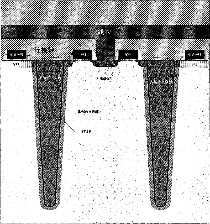
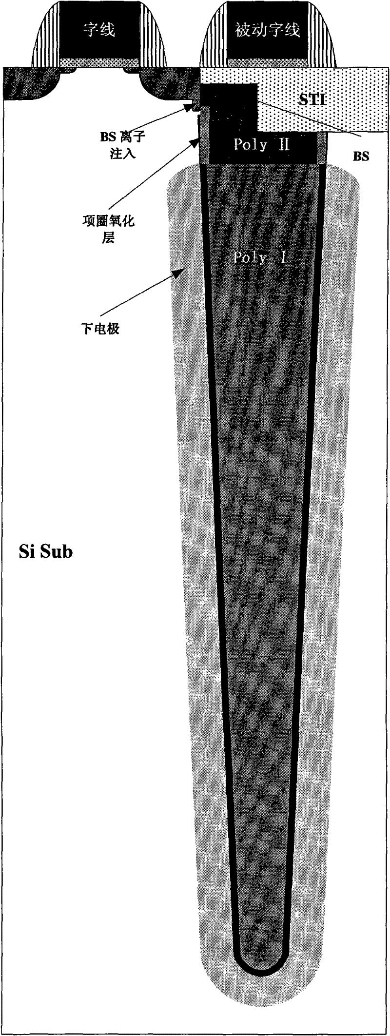
[0037] First see Figure 8 , This embodiment provides a DRAM structure with an extended trench on the basis of the process of using BEST to fabricate a buried connection strip, including an NMOS transistor 6 and a trench capacitor connected to its source.

[0038] Wherein, the trench capacitor includes:

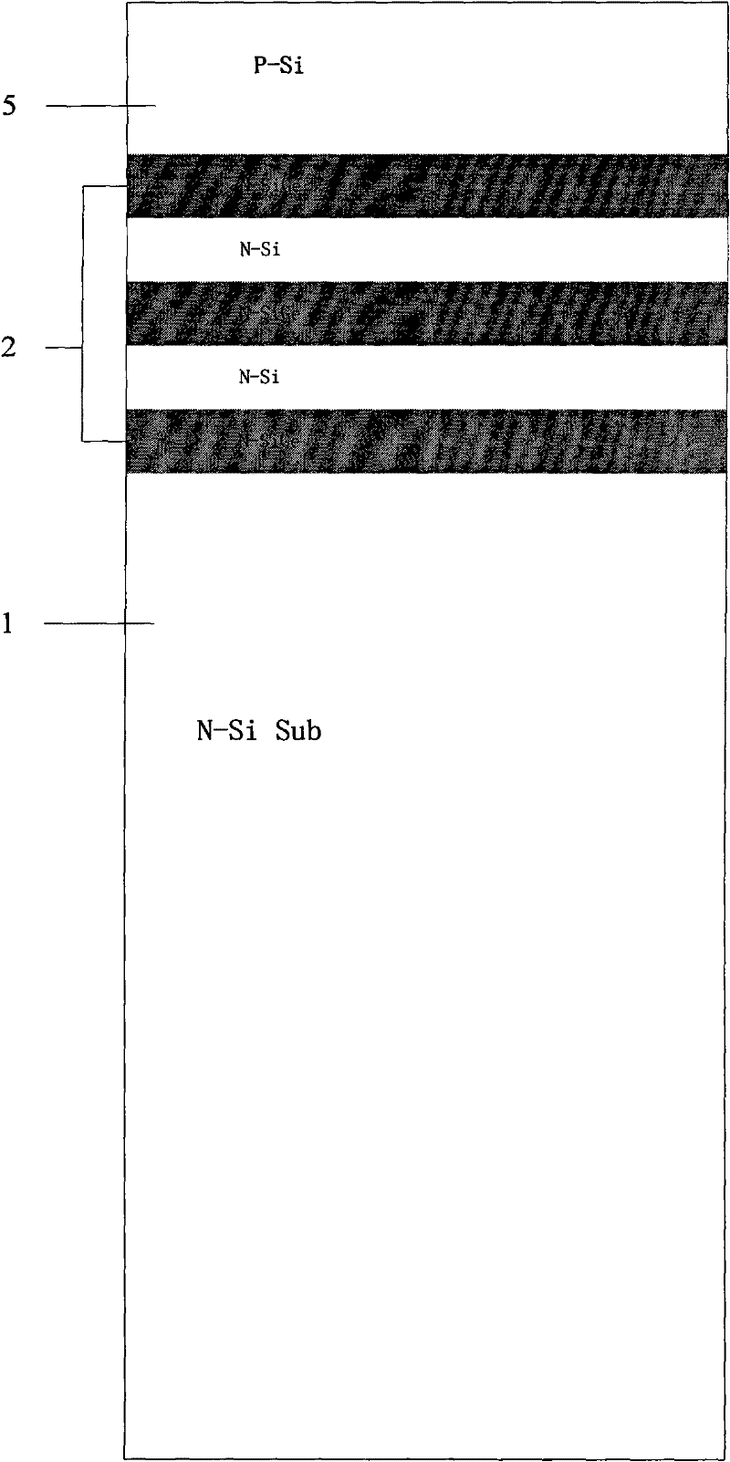
[0039] The semiconductor substrate can be either a P-type substrate or an N-type substrate. In this embodiment, an N-type Si substrate 1 is used as an example, so that it is the same as the SiGe / Si epitaxial stack;

[0040] The alternately arranged N-type SiGe layers and N-type Si layers 2 are located on the N-type Si substrate 1, and may be multiple layers. In this embodiment, for example Figure 8As shown, on the N-type Si substrate 1, a layer of N-type SiGe layer, a layer of N-type Si layer, another layer of N-type SiGe layer, and another layer of N-type Si layer are sequentially arranged in such an alternating upward direction;

[0041] The trench is located in the alte...

Embodiment 2

[0057] See Figure 9 , which is different from Embodiment 1 in that the uppermost layer of the alternately grown multilayer N-type SiGe layers and N-type Si layers is an N-type Si layer, and then a P-type Si layer is fabricated thereon.

[0058] In the present invention, the stacking order and number of layers of alternating N-type SiGe layers and N-type Si layers are not limited.


PUM


Abstract

The invention discloses a DRAM (Dynamic Random Access Memory) structure with an expansion groove and a manufacturing method thereof. The structure comprises an NMOS (N-channel Metal Oxide Semiconductor) transistor and a groove capacitor connected with a source electrode thereof, wherein the groove capacitor comprises a semiconductor substrate, an N-type SiGe layer and an N-type Si layer which arealternately arranged, a groove, a dielectric layer and a polysilicon layer, wherein the groove is located in the N-type SiGe layer and the N-type Si layer which are alternately arranged and extends into the semiconductor substrate, and the section of a side wall of the groove is in a comb tooth shape; the N-type SiGe layer and the N-type Si layer which are alternately arranged are utilized as a lower pole plate; the dielectric layer is located at the surface of the inner wall of the groove; the polysilicon layer is filled in the groove and utilized as an upper pole plate of the groove capacitor; a P-type Si layer is also prepared on the N-type SiGe layer and the N-type Si layer which are alternately arranged; and the NMOS transistor is manufactured on the P-type Si layer. Through the method, the N-type SiGe layer and the N-type Si layer are alternately grown by utilizing a doping and epitaxial technique and the side wall in the comb tooth shape is manufactured by utilizing selective etching; and the method improves the structure of a deep groove capacitor in the DRAM and simplifies the manufacturing process.

Description

technical field [0001] The invention relates to a dynamic random access memory (DRAM, Dynamic Random Access Memory) cell structure and a manufacturing process thereof, in particular to a DRAM cell structure with extended trenches and a manufacturing process thereof, belonging to the technical field of semiconductor manufacturing. Background technique [0002] At present, the industry generally adopts the structure of 1T1C (one transistor with one capacitor) as a DRAM unit. This combination of 1T1C components makes the storage bits of DRAM become the electronic components with the highest density and the lowest unit manufacturing cost, and has an irreplaceable position in computer access devices. With the rapid development of semiconductor technology, DRAM components are rapidly developing in the direction of high density and high capacity. One of the most important challenges in DRAM technology is how to design capacitors with comparable capacitances while the area per unit...

Claims


Application Information

Patent Timeline
Patent Type & Authority Patents(China)
IPC IPC(8): H01L27/108H01L21/8242
Inventor 黄晓橹陈静张苗王曦
Owner SHANGHAI INST OF MICROSYSTEM & INFORMATION TECH CHINESE ACAD OF SCI
Why Eureka
Try Eureka