Method for preparing photo-electrode

A technology of photoelectrodes and conductive substrates, applied in the field of solar photoelectric conversion, can solve the problems of unfavorable practical application of industrial production, complex operation of chemical deposition method, low photoelectric energy conversion efficiency, etc., to achieve improved photoelectric conversion efficiency, simple equipment and low production cost low effect

Inactive Publication Date: 2011-04-13
PEKING UNIV
View PDF1 Cites 22 Cited by
  • Summary
  • Abstract
  • Description
  • Claims
  • Application Information

AI Technical Summary

Problems solved by technology

Oxide semiconductors are generally wide bandgap semiconductors (Eg≥3.0eV), which have good photostability, but the problem is that the photoelectric energy conversion efficiency is low
Chinese patent application publication CN101393938A discloses a photoelectrode, which uses chemical deposition to fill narrow-bandgap quantum dots into wide-bandgap semiconductor nanotube / line array films, thereby improving its photoelectric conversion efficiency, but the operation of chemical deposition is complicated , the reaction conditions are not easy to control, which is not conducive to the practical application in industrial production
However, the technology of introducing sensitizers into oxide semiconductor nanoarray films by near-space sublimation method to prepare photoelectrodes has not been reported, and the control of factors such as temperature and pressure during the deposition process still needs further research.

Method used


Image

  • Method for preparing photo-electrode
  • Method for preparing photo-electrode
  • Method for preparing photo-electrode

Examples


Embodiment Construction

[0020] Below in conjunction with accompanying drawing, the present invention is described in further detail through the embodiment, but the present invention is not limited in any way.

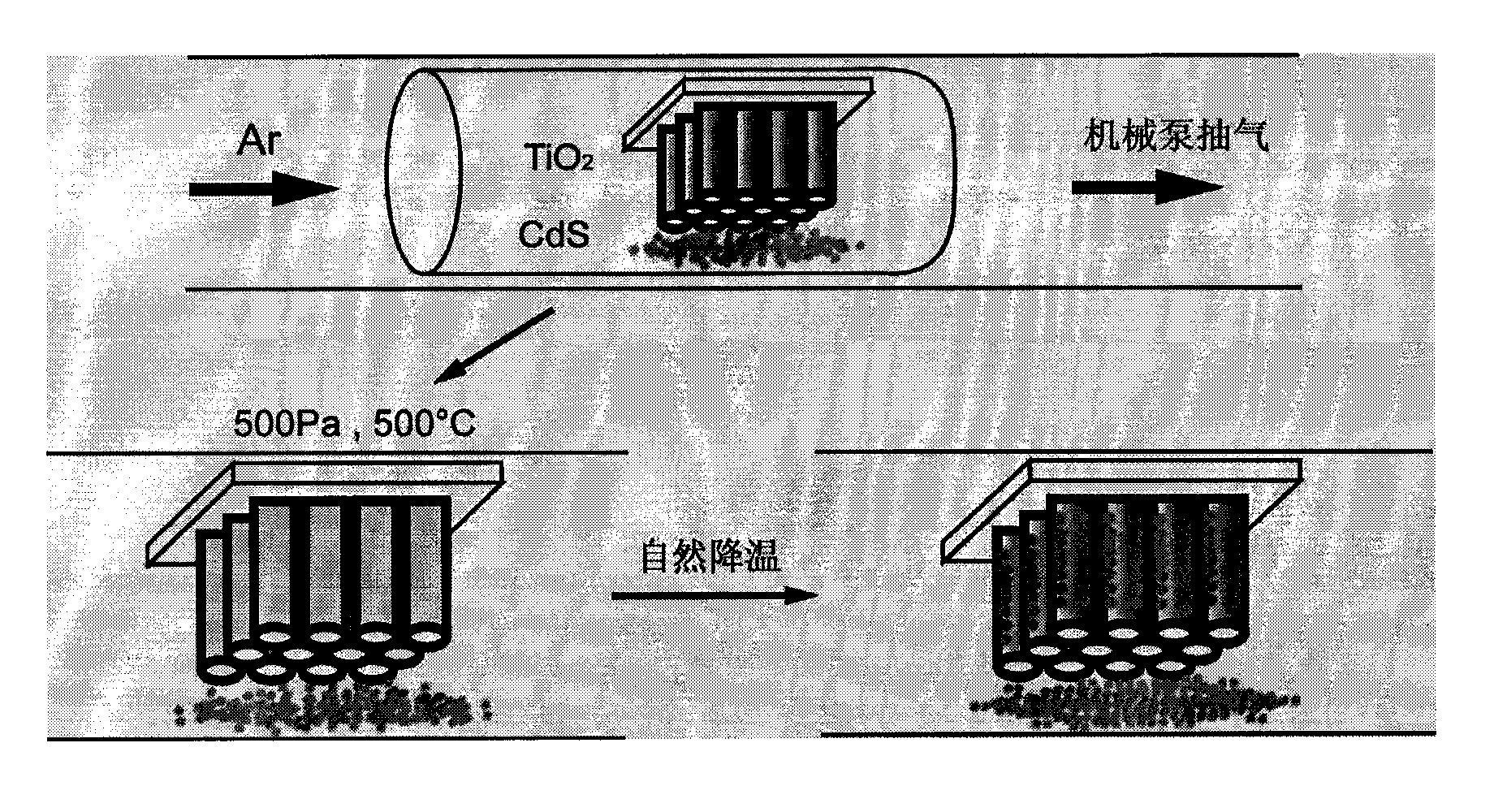
[0021] Taking the preparation of cadmium sulfide / titanium dioxide heterojunction photoelectrode as an example, the following steps are included:

[0022] (1) Utilize the method for anodic oxidation to obtain titanium dioxide nanotube array on a conductive substrate;

[0023] (2) in the quartz tube of the tube furnace, the titanium dioxide nanotube array opening prepared in step (1) is suspended above the cadmium sulfide powder downward;

[0024] (3) Feed argon to clean the quartz tube twice, and adjust the air pressure of the system between 500Pa-600Pa under an argon atmosphere;

[0025] (4) Heat the system to 500°C. As the temperature increases, cadmium sulfide becomes gaseous and infiltrates into the titanium dioxide nanotube array, and reaches a saturated state;

[0026] (5) After 15-25 m...


PUM

PropertyMeasurementUnit
strengthaaaaaaaaaa

Abstract

The invention discloses a method for preparing a photo-electrode, which comprises the steps of: firstly preparing a wide band-gap semiconductor nanotube or nano-wire array on a conductive substrate, and then filling narrow band-gap semiconductor nano particles into the wide band-gap semiconductor nanotube or nano-wire array by the close-spaced sublimation method in presence of decompression, thereby obtaining a narrow band-gap semiconductor and a wide band-gap semiconductor heterojunction film photo-electrode. The narrow band-gap semiconductor nano particles strengthen the response of a wide band-gap semiconductor nano array film to visible lights, the absorption of the photo-electrode to the visible lights is greatly enhanced, and therefore the photoelectric conversion efficiency is improved. Furthermore, equipment required by the close-spaced sublimation method is simple and easy for operation and has low production cost, therefore, the method for preparing the photo-electrode is suitable for being popularized and applied widely.

Description

technical field [0001] The invention belongs to the field of photoelectric conversion of solar energy, and relates to a photoelectrode using a wide bandgap semiconductor nanotube / line array film, in particular to a method for improving its photoelectric conversion efficiency by using a narrow bandgap semiconductor material. Background technique [0002] At present, in the field of photoelectrochemical solar cell research, the use of nanoscale oxide semiconductor materials such as TiO 2 , ZnO, SnO 2 As a photoelectrode, it has become a research hotspot because of its good application prospects, among which nano-TiO 2 It has become the most commonly used material because of its cheap, stable, and non-toxic advantages. Oxide semiconductors are generally wide bandgap semiconductors (Eg≥3.0eV), which have good photostability, but the problem is that the photoelectric energy conversion efficiency is low. Studies have shown that the titanium dioxide nanotube array structure has ...

Claims


Application Information

Patent Timeline
Patent Type & Authority Applications(China)
IPC IPC(8): H01G9/042H01G9/20H01M14/00H01L31/18H01L31/0224
CPCY02P70/50
Inventor 孙文涛彭练矛高显峰
Owner PEKING UNIV
Why Eureka
Try Eureka