Heating tool in semiconductor encapsulating and routing process and method thereof

A heating method and semiconductor technology, applied in semiconductor devices, semiconductor/solid-state device manufacturing, electric solid-state devices, etc., can solve the problems of increasing the temperature of the chip holder 112, damage to the welding pad 131, etc.

Inactive Publication Date: 2013-03-27
ASE ASSEMBLY & TEST SHANGHAI
View PDF2 Cites 0 Cited by
  • Summary
  • Abstract
  • Description
  • Claims
  • Application Information

AI Technical Summary

Problems solved by technology

[0005] However, the design of the heating fixture of the lead frame has the following disadvantages: since the heating block 12 is integrally formed, the chip holder 112 is also increased when the inner pin part 111a is heated. temperature, and jointly heated the bonding pad 131 of the semiconductor chip 13
However, the one-piece design of the heating block 12 of the heating fixture of the substrate is also easy to overheat the solder pads 131 of the semiconductor chip 13 to make them excessively softened, thus causing disadvantages such as damage to the solder pads 131 during wire bonding.

Method used


Image

  • Heating tool in semiconductor encapsulating and routing process and method thereof
  • Heating tool in semiconductor encapsulating and routing process and method thereof
  • Heating tool in semiconductor encapsulating and routing process and method thereof

Examples


Embodiment Construction

[0031] In order to make the above-mentioned purposes, features and advantages of the present invention more obvious and understandable, the preferred embodiments of the present invention will be specifically cited below, together with the accompanying drawings, for a detailed description as follows:

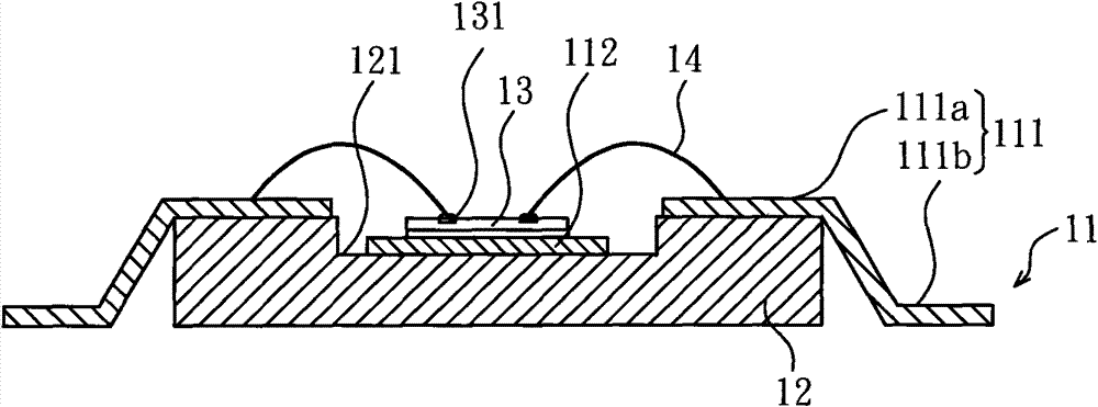
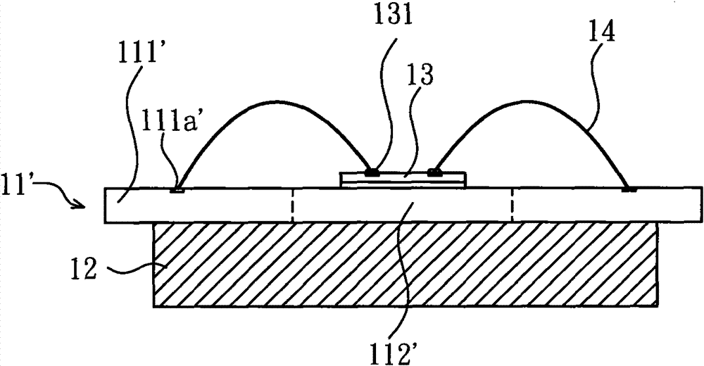
[0032] The heating jig and method thereof in the semiconductor packaging wire bonding process provided by the present invention are mainly used for temporarily carrying and actively heating / cooling packaging carriers such as leadframes or substrates during the wire bonding process, so as to improve The quality of the wire bonding.

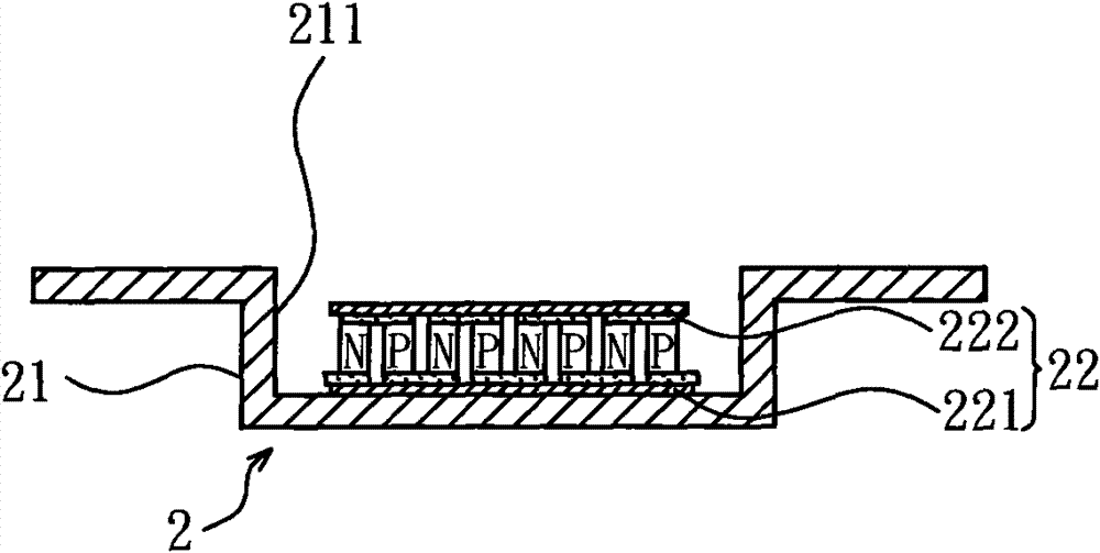
[0033] Please refer to image 3 and 4 As shown, the heating fixture 2 in the semiconductor package wire bonding process according to the first embodiment of the present invention mainly includes: a heating block 21 and an active cooling element 22 . The heating block 21 is a metal block, and its material can be copper, iron, aluminum, nickel or allo...


PUM


Abstract

The invention discloses a heating tool in a semiconductor encapsulating and routing process and a method thereof. A heating block of the heating tool is matched with an active refrigeration element and can heat a first region of an encapsulating carrier, and the refrigeration surface of the active refrigeration element can actively reduce the temperature of a second region of the encapsulating carrier to be relatively lower than the temperature of the first region so that the welding pad hardness of a chip in the second region can be kept at a suitable preset hardness value and favorably improve the bonding reliability and the bonding yield between leads and the welding pad.

Description

【Technical field】 [0001] The present invention relates to a heating jig and its method in the wire bonding process of semiconductor packaging, in particular to a fixture used for temporary loading and active heating / cooling in the wire bonding process of semiconductor packaging during the wire bonding process. Heating jig and method thereof. 【Background technique】 [0002] The semiconductor packaging process is used to provide a packaging structure to protect a semiconductor chip, so that the semiconductor chip can avoid external force impact, dust pollution, moisture or oxidation when it is powered on, so that the packaging structure can be used to improve the reliability of the semiconductor chip and prolong the life of the semiconductor chip. its service life. In the existing manufacturing process of semiconductor packaging, semiconductor wafers are usually obtained first and wafer tests are performed on them. After passing the test, the semiconductor wafers will then be...

Claims


Application Information

Patent Timeline
Patent Type & Authority Patents(China)
IPC IPC(8): H01L21/00H01L21/60
CPCH01L2924/15311H01L2224/48091H01L2224/73265H01L2224/32245H01L2224/48247H01L2224/45147H01L2224/45144H01L2924/01015H01L2924/01047H01L2924/181
Inventor 王德峻吕岱烈
Owner ASE ASSEMBLY & TEST SHANGHAI
Why Eureka
Try Eureka