A growth method of a light-emitting composite layer and an LED epitaxial structure containing the structure

A technology of epitaxial structure and growth method, which is applied in the direction of electrical components, circuits, semiconductor devices, etc., can solve the problems that the brightness and antistatic ability cannot meet the actual needs, the crystallization quality of the light-emitting area is reduced, and the antistatic ability is not high, so as to reduce the Effects of lattice defects, enhancement of confinement, and improvement of antistatic ability

Active Publication Date: 2018-08-21
XIANGNENG HUALEI OPTOELECTRONICS
View PDF4 Cites 0 Cited by
  • Summary
  • Abstract
  • Description
  • Claims
  • Application Information

AI Technical Summary

Problems solved by technology

[0017] In the existing LED epitaxial structure, the lattice mismatch and dislocations at the bottom can easily enter the low-temperature quantum well region, resulting in a decrease in the crystal quality of the light-emitting region and an increase in defects. The recombination layer cannot effectively prevent defects and dislocations from the bottom from entering the low-temperature quantum well region, which will lead to a serious decline in the crystal quality of the light-emitting region, and the antistatic ability is naturally not high; the polarization effect is more obvious, and electrons and holes undergo radiative recombination The efficiency is passively decreased, so the low brightness is also a natural thing
[0018] At present, the market has higher and higher requirements for the brightness and antistatic ability of LED chips, but the brightness and antistatic ability of the existing LED epitaxial structure still cannot meet the actual needs. Therefore, a new LED epitaxial structure is urgently needed in the industry To solve the deficiencies of the existing technology

Method used


Image

  • A growth method of a light-emitting composite layer and an LED epitaxial structure containing the structure
  • A growth method of a light-emitting composite layer and an LED epitaxial structure containing the structure
  • A growth method of a light-emitting composite layer and an LED epitaxial structure containing the structure

Examples


Embodiment 1

[0061] Aixtron MOCVD is used to grow high-brightness GaN-based LED epitaxial wafers, specifically: high-purity H 2 or high purity N 2 or high purity H 2 and high purity N 2 The mixed gas as the carrier gas, high-purity NH 3 As the N source, the metal-organic source trimethylgallium (TMGa) is used as the gallium source, triethylgallium (TEGa) is used as the gallium source, trimethylindium (TMIn) is used as the indium source, and the N-type dopant is silane (SiH 4 ), trimethylaluminum (TMAl) as the source of aluminum, and the P-type dopant as magnesium dicene (CP 2 Mg), the substrate is sapphire, and the reaction pressure is between 100mbar and 800mbar.

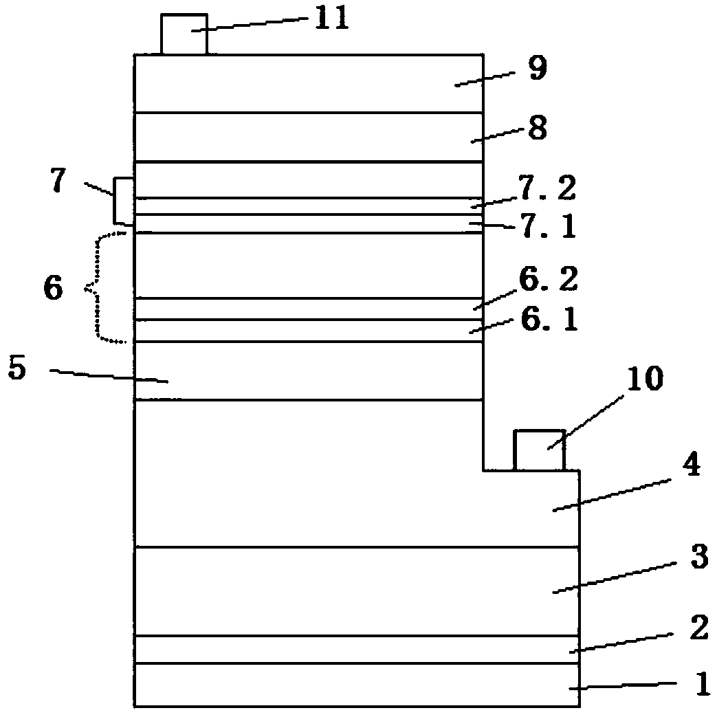
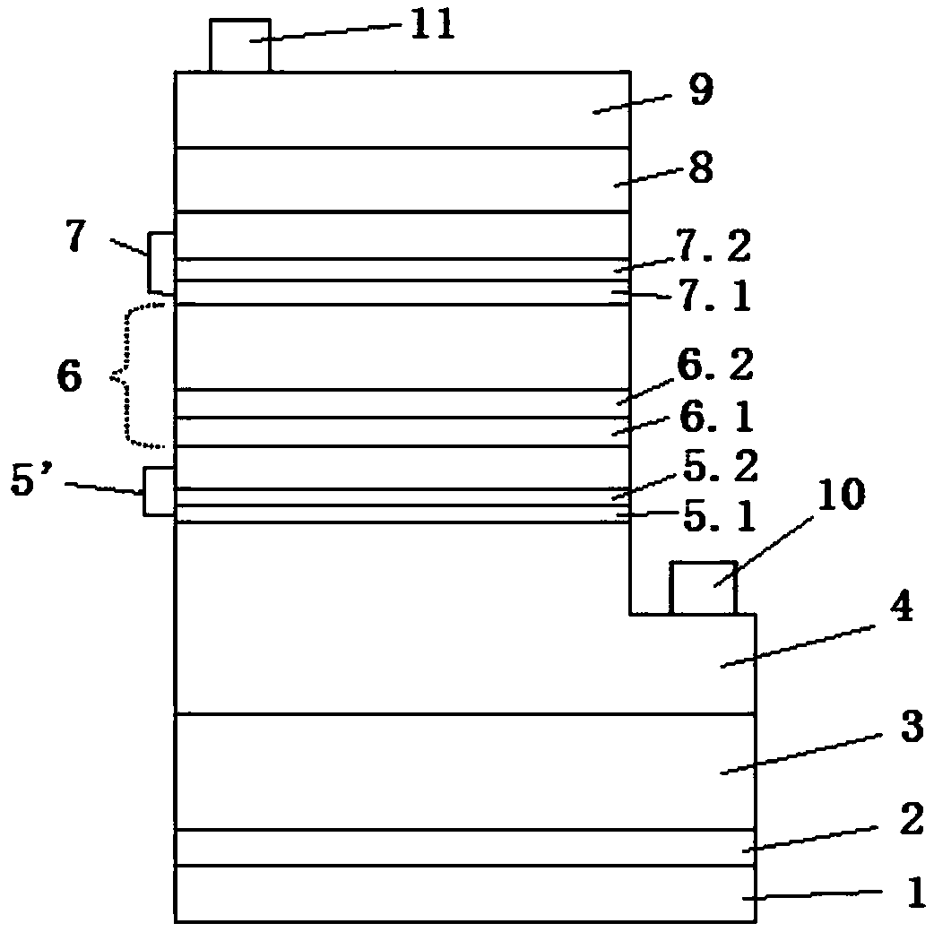
[0062] An LED epitaxial structure, see figure 2, including the following structure: from bottom to top, it includes sapphire substrate 1, low-temperature buffer layer 2, undoped GaN layer 3, Si-doped N-type GaN layer 4, light-emitting composite layer 5', light-emitting layer 6, superlattice layer 7, a first Mg-doped P-ty...

Embodiment 2

[0088] The only difference from Embodiment 1 is: the number of single pieces included in the optical composite layer 5', and the number of single pieces in this embodiment is 9.

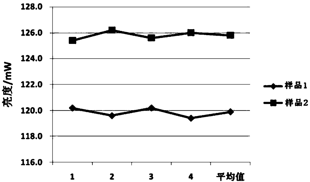
[0089] Sample 1 was prepared according to the existing LED growth method (see background art for details), and sample 2 and sample 3 were prepared according to the method of the present invention (Example 1-2). Samples 1-3 were plated with an ITO layer of about 150nm under the same pre-process conditions, plated with a Cr / Pt / Au electrode of about 70nm under the same conditions, and plated a protective layer of SiO under the same conditions 2 About 30nm, and then grind and cut the sample into (16mil*33mil) chip particles under the same conditions, and then test the photoelectric performance of samples 1-3 on the same testing machine, see brightness comparison for details image 3 , see the comparison of antistatic ability Figure 4 , because the effects of sample 3 and sample 2 are equivalent, so onl...


PUM

PropertyMeasurementUnit
thicknessaaaaaaaaaa
thicknessaaaaaaaaaa
thicknessaaaaaaaaaa

Abstract

The first purpose of the invention lies in disclosing a growing method for a light-emitting composite layer, and the method comprises the steps: periodically growing 8-9 wafers, wherein each wafer sequentially comprises a first InxGa(1-x)N layer and a first GaN layer from the bottom to the top, wherein x=0.15-0.25. The second purpose of the invention lies in providing an LED epitaxial structure comprising the light-emitting composite layer. The light-emitting composite layer (a high-temperature quantum well structure) can achieve the absorption of lattice mismatch and dislocation at the bottom of an epitaxial layer and the relief of an internal stress, thereby reducing the lattice defects of a low-temperature quantum well, protecting the low-temperature quantum well to great extent, improving the crystal quality of a light-emitting region, and improving the anti-static capability of the LED epitaxial structure. Meanwhile, the structure employs a mode of low-temperature growing, can greatly reduce the separate-out of In, achieves the improvement of the confinement of carriers, increases the number of light-emitting quantum dots, facilitates the improvement of radiative recombination efficiency, and improves the light-emitting intensity.

Description

technical field [0001] The invention relates to the technical field of LEDs, in particular to a method for growing a light-emitting composite layer and an LED epitaxial structure containing the structure. Background technique [0002] At present, LED is a kind of solid-state lighting, which has the advantages of small size, low power consumption, long service life, high brightness, environmental protection, durability, etc., and is deeply loved by consumers. With the gradual expansion of the scale of domestic production of LEDs, the demand for LED light effects in the market is increasing day by day. [0003] Gallium nitride-based materials (including InGaN, GaN and AlGaN alloys) are direct bandgap semiconductors, and their bandgap is continuously adjustable from 0.7-6.2eV. They have excellent properties such as wide direct bandgap, strong chemical bonds, high temperature resistance, and corrosion resistance. , is an ideal material for the production of short-wavelength hig...

Claims


Application Information

Patent Timeline
Patent Type & Authority Patents(China)
IPC IPC(8): H01L33/00
CPCH01L33/007
Inventor 郭嘉杰徐迪
Owner XIANGNENG HUALEI OPTOELECTRONICS
Why Eureka
Try Eureka