Composite materials having substrates with self-assembled colloidal crystalline patterns thereon

a technology of colloidal crystals and composite materials, which is applied in the direction of traffic signals, instruments, roads, etc., can solve the problems of inability of light to propagate in the photonic crystal at wavelengths corresponding to pbg, the gap between the photonic band and the pbg, and the research is still in its infancy, and achieves the effect of photonics

Inactive Publication Date: 2006-05-16
THE GOVERNINIG COUNCIL OF THE UNIV OF TORANTO
View PDF9 Cites 36 Cited by
  • Summary
  • Abstract
  • Description
  • Claims
  • Application Information

AI Technical Summary

Benefits of technology

[0019]It is an object of the present invention to provide methods for synthesizing patterned colloidal crystals on the surfaces of, or embedded in, substrate

Problems solved by technology

This leads to the development of a photonic band gap (PBG) in the photon density of states (PDS) and the inability of light to propagate in the photonic crystal at wavelengths corresponding to the PBG.
These effects include the localization of light and inhibition of spontaneous emission, however this research is still in its infancy.
This is mainly because of the technical difficulty of producing well ordered three-dimensional structures having dielectric periodicity on the order of the wavelength of visible and near infrared light.
A significant obstacle to the realization of these photonic capabilities is the lack of a proven route for synthesis of high quality, very large-scale PBG materials and patterns thereof with significant electromagnetic gaps at micron and sub-micron wavelengths.
Not surprisingly, technologies founded on photonic crystals are presently facing scientific challenges like those confronted with semiconductors in the 1940's and 1950's.
Physical methods of shaping bulk semiconductors into photonic crystals involve complex, time consuming and expensive multi-step processing.
The method is time c

Method used


Image

  • Composite materials having substrates with self-assembled colloidal crystalline patterns thereon
  • Composite materials having substrates with self-assembled colloidal crystalline patterns thereon
  • Composite materials having substrates with self-assembled colloidal crystalline patterns thereon

Examples


example 4

Spin-coating Colloidal Crystal Clusters Inside Square Pyramid-shaped Pits in Silicon (100) Wafers

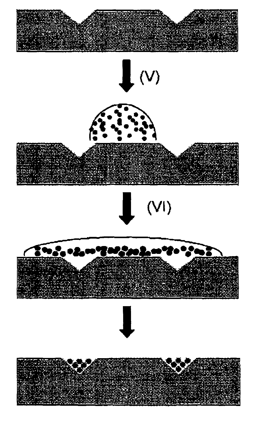
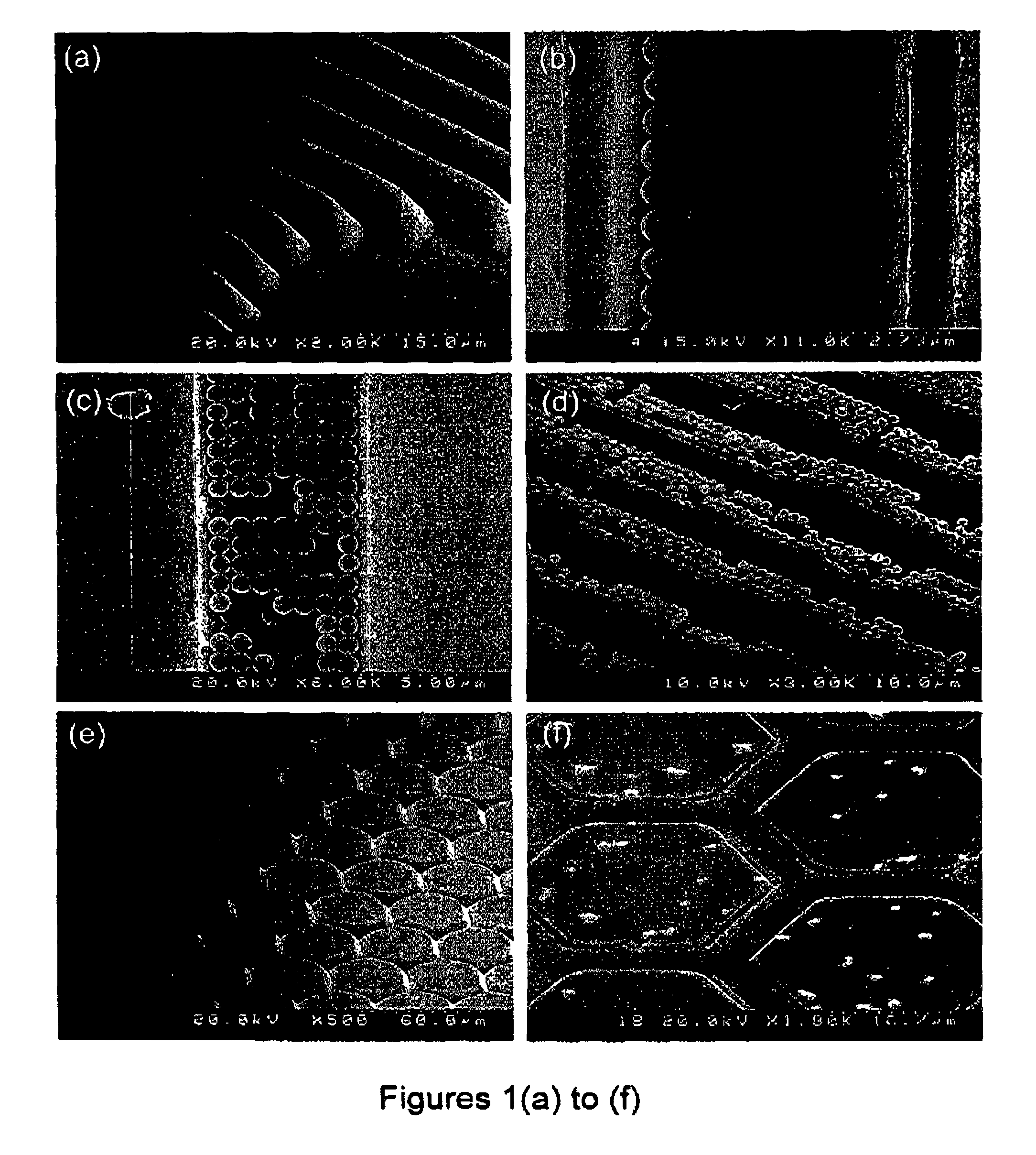
[0152]Interestingly, the first micro-spheres observed to nucleate in the square pyramidal-shaped etch pits are singlet, duplet, triplet and quadruplet and so forth type arrangements of micro-spheres located at the apex of the square pyramid pit, some examples being shown in FIGS. 5a, 5b, 6c. These embryonic micro-sphere clusters are found to dominate in the early stages of the spin-coating, colloidal self-assembly process inside the silicon etch pits and when dilute aqueous dispersions of micro-spheres are used. At later stages and with more concentrated dispersions, microspheres close-pack always starting from the apex and continue to grow up the walls and along the edges of the square pyramid-shaped etch pit to eventually fill them with well-ordered patterns of colloidal crystals, FIG. 6a. The edges of the pits generally seem to be filled first with well-ordered micro-spheres and the s...

example 5

Spin-coating Single Crystal Colloidal Crystals Inside Rectangular Pyramid-shaped Pits in Silicon (100) Wafers

[0155]Another attractive and inventive feature of the spin-coating process of this disclosure is the ability to intentionally tune the orientation and lattice structure of the colloidal crystal grown within the etch pits inside the wafer. This observation stems from the effect of the geometry of the etch pits on the nucleation and growth of the colloidal crystal within. A rectangular pyramid-shaped etch pit can be used to illustrate this novel and inventive concept reduced to practice in this disclosure. Because the first micro-spheres to settle in a rectangular pyramid-shaped etch pit most likely settle on the apex line, the number and geometry of this embryonic micro-sphere arrangement depends on the relative sizes of the micro-sphere diameter and the length of the line that defines the apex of the rectangular pyramid-shaped pit. If the arrangement is commensurate, that is ...

example 3

Modulated Thickness Colloidal Crystal Micro-channels

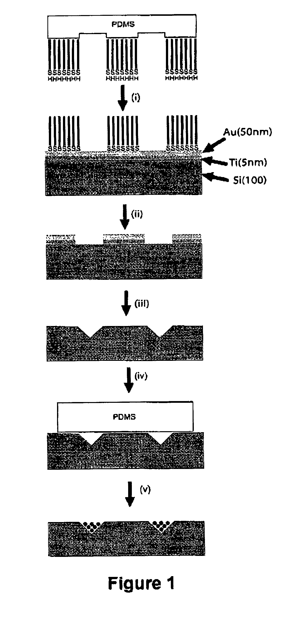
[0190]The grooves described in this example have designed thickness controlled either by etching time of silicon wafer or the thickness of a relief structure in a photo-resist pattern. A method to prepare a vertical wall micro-channel with modulated depth is described herein. FIG. 27 illustrates a procedure for the fabrication of a modulated thickness colloidal crystal. The procedure is similar to the preparation of the wood-pile structure, FIG. 25a. During the heating step for transferring the pattern to the substrate, the oven temperature is set at 180° C., which is higher than the glass transition temperature of the PMMA. The PMMA line structure imprints its pattern on the POMS stamp. By putting this imprinted PDMS stamp on a flat substrate, followed by capillary infiltration of polyurethane (NOA73, Norland) and curing under UV light, a line pattern with modulated steps is formed. After removing the PDMS, the patterned substrate...


PUM


Abstract

Composite materials having colloidal photonic crystals patterned in substrates for use in different technologies including lab-on-chip and photonic chip technologies. The colloidal crystals are patterned either on or within surface relief patterns in the substrates of the composite materials and each colloidal crystal exhibits Bragg diffraction.

Description

CROSS REFERENCE TO RELATED U.S. PATENT APPLICATIONS[0001]This patent application relates to U.S. provisional patent application Ser. No. 60 / 240,055 filed on Oct. 16, 2000 entitled METHOD OF SELF-ASSEMBLY OF CRYSTALLINE COLLOIDAL PATTERNS ON SUBSTRATES, Ser. No. 60 / 253,081 filed on Nov. 28, 2000 entitled METHOD OF SELF-ASSEMBLY OF CRYSTALLINE COLLOIDAL PATTERNS ON SUBSTRATES, and Ser. No. 60 / 296,119 filed on Jun. 7, 2001 entitled METHOD OF SELF-ASSEMBLY OF CRYSTALLINE COLLOIDAL PATTERNS ON SUBSTRATES.FIELD OF THE INVENTION[0002]The present invention relates to methods of synthesis and optical applications of composite materials comprised of crystalline colloidal patterns on substrates, and more particularly the present invention is related to a method of synthesizing crystalline photonic crystals on the surfaces of, or embedded within, substrates and optical utility thereof.BACKGROUND OF THE INVENTION[0003]Photonics is the science of molding the flow of light. A photonics revolution ...

Claims


Application Information

Patent Timeline
IPC IPC(8): C30B7/02A61F2/01G02B6/12B05D1/28B32B3/30B32B9/00G02B6/122G02B6/13
CPCB32B9/00B82Y20/00B82Y40/00G02B6/1225G02B6/13B32B3/30B05D1/283Y10T428/24355B82Y15/00B82Y30/00Y10S977/779Y10S977/883Y10T428/24479Y10T428/2462Y10T428/24579Y10T428/24372Y10T428/2457
Inventor OZIN, GEOFFREY ALANYANG, SAN MINGMIGUEZ, HERNAN
Owner THE GOVERNINIG COUNCIL OF THE UNIV OF TORANTO
Why Eureka
Try Eureka