Linear array semiconductor laser with photonic crystal structure

A technology of photonic crystals and two-dimensional photonic crystals, which is applied in the direction of semiconductor lasers, lasers, phonon exciters, etc., can solve the problems of difficult preparation process, few light-emitting points, and high series resistance

Inactive Publication Date: 2011-04-13
CHANGCHUN UNIV OF SCI & TECH
View PDF3 Cites 0 Cited by
  • Summary
  • Abstract
  • Description
  • Claims
  • Application Information

AI Technical Summary

Problems solved by technology

[0005] The purpose of the present invention is to solve the problems of the existing laser linear array with few light emitting points, large horizontal output divergence angle, high series resistance, poor thermal stability, and difficult preparation process. The present invention provides a laser with a photonic crystal structure. The structure and process method of linear array semiconductor lasers, which can greatly increase the number of light-emitting units of linear array lasers, increase the output power of linear arrays of lasers, improve the beam quality of device-level output, reduce the series resistance of array devices, and improve device arrays. Linearity, improved thermal stability of the device

Method used


Image

  • Linear array semiconductor laser with photonic crystal structure
  • Linear array semiconductor laser with photonic crystal structure

Examples


specific Embodiment approach 1

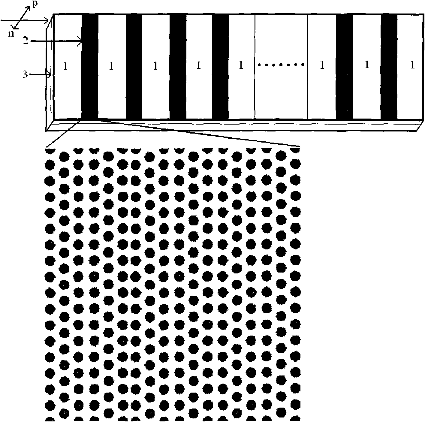
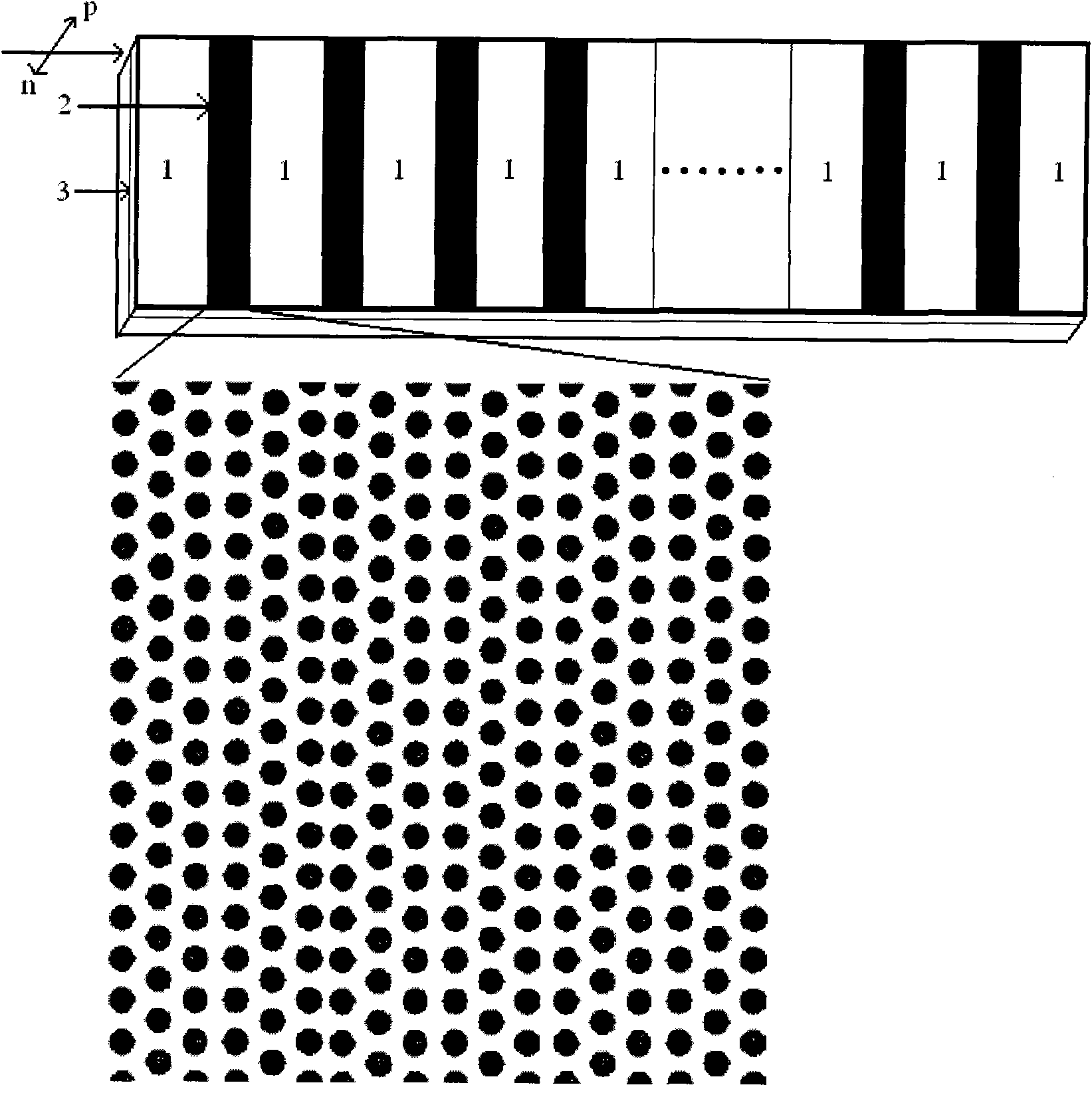
[0015] Specific implementation mode one: see figure 1 As shown, the linear array semiconductor laser structure of photonic crystal structure includes laser epitaxial wafer n-plane structure region, p-plane structure region, active region, two-dimensional photonic crystal distribution region, p-plane current injection region, n-face electrode, p-plane The electrode and the photonic crystal distribution area are composed of an air-hole photonic crystal structure on the semiconductor material, and the photonic crystal structure is used as a mode selection area of ​​a linear array laser and a lateral light isolation area.

specific Embodiment approach 2

[0016] Embodiment 2: The etching depth of holes in the two-dimensional photonic crystal area is 0.8-1.2 microns, and the bottom and side walls of the holes are sequentially attached with titanium, platinum, and gold p-surface electrode materials.

specific Embodiment approach 3

[0017] Embodiment 3: The difference between this embodiment and Embodiment 2 is that the etching depth of the holes in the two-dimensional photonic crystal region is 1.2-5 microns, and the bottom and side walls of the holes are covered with aluminum oxide or aluminum nitride or silicon dioxide. an insulating medium layer, and on the insulating medium layer are titanium, platinum, and gold p-surface electrode materials in sequence.


PUM


Abstract

The invention relates to a linear array semiconductor laser with a photonic crystal structure, and belongs to the technical field of semiconductor photo-electronic devices. The characteristics of the specific structure of a two-dimensional photonic crystal material such as mode selection property of a specific light field, light isolation of a specific direction and the like are utilized, and the light isolation structure of the traditional linear array semiconductor laser is replaced by using the two-dimensional photonic crystal structure, so the luminous area of the linear array semiconductor laser is increased, the output power of the device is improved, the beam quality and the luminous efficiency of the output of the device in the horizontal direction are improved, the series resistance of the device is reduced, and the thermal stability and the output property of the device are improved. The technical scheme is suitable for manufacturing the linear array high-power semiconductor lasers of various wavelengths.

Description

technical field [0001] The invention relates to a linear array semiconductor laser with a photonic crystal structure. technical background [0002] Linear array semiconductor laser is a linear array of semiconductor lasers. It has the characteristics of large output power, small size, long life, and good beam quality. It has gradually become the mainstream of laser applications and is moving towards higher output power and higher output. Character development. [0003] The traditional linear array semiconductor laser is limited by the traditional technology and its own working characteristics. It is required that the optical oscillation in the direction of the linear array should be well suppressed. It is difficult for the traditional structure to achieve the design of high-density light-emitting points, and the linearity of the far-field light point distribution These disadvantages reduce device output, thermal stability, and fiber coupling efficiency. In particular, the ...

Claims


Application Information

Patent Timeline
Patent Type & Authority Applications(China)
IPC IPC(8): H01S5/18H01S5/323
Inventor 乔忠良张斯钰薄报学高欣李辉王玉霞李占国芦鹏王勇李特李再金邹永刚李林刘国军
Owner CHANGCHUN UNIV OF SCI & TECH
Why Eureka
Try Eureka