
Method for preparing large-size GaN self-support substrate

A self-supporting substrate, large-scale technology, applied in chemical instruments and methods, from chemically reactive gases, single crystal growth, etc., can solve problems such as lower yield, expensive laser lift-off technology, and affect device quality

Inactive Publication Date: 2011-04-27
INST OF SEMICONDUCTORS - CHINESE ACAD OF SCI
View PDF0 Cites 8 Cited by
  • Summary
  • Abstract
  • Description
  • Claims
  • Application Information

AI Technical Summary

Problems solved by technology

However, the laser lift-off technology is expensive; and in the process of laser lift-off, the high-pressure gas generated after the GaN pyrolysis at the interface is easy to cause damage to the prepared GaN self-supporting substrate, and at least a large number of sites are generated on the GaN self-supporting substrate. Errors and microcracks will affect the quality of future devices, and in severe cases, the GaN self-supporting substrate will be completely broken, which will greatly reduce the yield

Method used


Image

  • Method for preparing large-size GaN self-support substrate
  • Method for preparing large-size GaN self-support substrate
  • Method for preparing large-size GaN self-support substrate

Examples


Embodiment 1

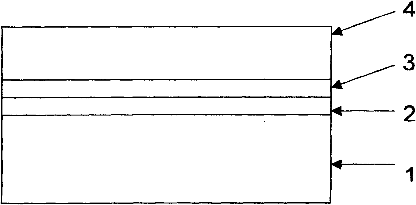
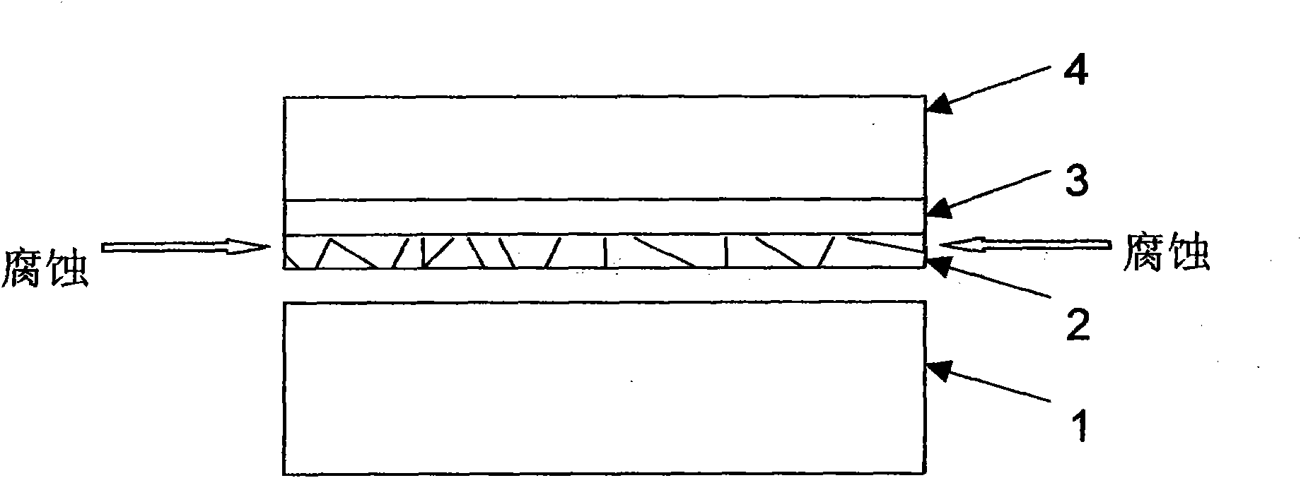
[0030] see figure 1 , figure 2 As shown, a method for preparing a large-scale GaN self-supporting substrate comprises the following steps:

[0031] Step 1: first grow a layer of ZnO film 2 on the substrate 1; wherein the materials for the substrate 1 for epitaxial self-supporting GaN thick film 4 are: sapphire, spinel, GaN, AlN, GaAs, Si , SiC, LiAlO 2 , LiGaO 2 , ZrB 2 or HfB 2 A kind of in, this example selects sapphire as substrate; Wherein the growth of ZnO film 2 adopts the method for metal source vapor phase epitaxy in this example, the source material that adopts in this method is metallic zinc and deionized water, metallic zinc and The reaction equation for deionized water is: This reaction is a reversible reaction. By constantly removing the tail gas and adjusting the flow rate of the source material and carrier gas, the reaction is controlled to achieve a dynamic balance, so that the metal Zn and H 2 O continuously reacts. The advantages of this method are ...

Embodiment 2

[0036] see again figure 1 , figure 2 Shown, present embodiment 2 is basically the same as embodiment 1, and its difference is:

[0037] (1) The ZnO film 2 in step 1 is prepared by spray pyrolysis, and the prepared ZnO film 2 is a polycrystalline film with a thickness of 0.5 μm. The advantage of the spray pyrolysis method is that the growth temperature is low, the method is simple, and the cost is very low.

[0038] (2) In step 2, a metal-organic chemical vapor deposition method is used to grow a 500nm InGaN film at 600°C as a low-temperature buffer layer; the InGaN low-temperature buffer layer 3 helps to reduce the defect density of the GaN thick film 4, and improves the final result. Crystalline quality of large-scale GaN free-standing substrates.

[0039] (3) High temperature corrosive gases HCl and NH in the hydride vapor phase epitaxy system during high temperature growth 3 pass figure 2 The direction indicated by the arrow etches the ZnO film 2 from the side. Becau...


PUM

PropertyMeasurementUnit
Thicknessaaaaaaaaaa
Thicknessaaaaaaaaaa

Abstract

The invention relates to a method for preparing a large-size GaN self-support substrate, which comprises the following steps of: 1. firstly, growing a layer of ZnO membrane on a substrate; 2. growing a low-temperature buffer layer on the ZnO membrane to form a sample; 3. growing a GaN thick membrane on the low-temperature buffer layer at high temperature in a hydride vapour phase epitaxy system; and 4. after growing in the hydride vapour phase epitaxy system at high temperature, directly separating the GaN thick membrane from the substrate to form a large-size GaN self-support substrate because corrosive gases, such as HCL, NH3, and the like in the hydride vapour phase epitaxy system corrodes the ZnO membrane.

Description

technical field [0001] The invention relates to a method for preparing a large-scale GaN self-supporting substrate by using methods such as hydride vapor phase epitaxy. Background technique [0002] The third-generation semiconductor materials represented by GaN and its alloys are new semiconductor materials that have received much attention in the world in the past decade. It has a large band gap, high electron saturation drift speed, small dielectric constant, good thermal conductivity, With many excellent properties such as stable structure, it has great application prospects in the fields of optoelectronics and microelectronics technology. In the field of optoelectronics, since the bandgap of III-nitrides is continuously adjustable in the range of 0.7-6.2eV, covering the band from red to ultraviolet, green, blue and even ultraviolet light-emitting devices and white lighting can be produced. In addition, the recently emerging UV LEDs have also shown special uses in scree...

Claims


Application Information

Patent Timeline
IPC IPC(8): C30B25/02C30B29/38
Inventor 胡强段瑞飞魏同波杨建坤霍自强曾一平
Owner INST OF SEMICONDUCTORS - CHINESE ACAD OF SCI
Learn More