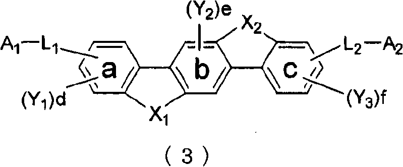
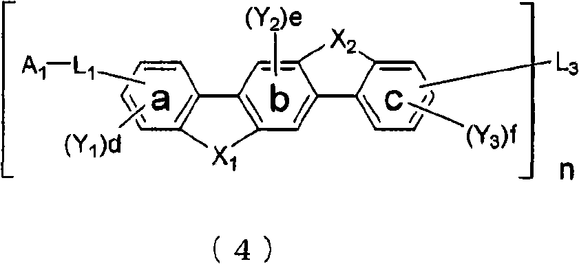
Halogen compound, polycyclic compound, and organic electroluminescence element comprising the polycyclic compound
A compound and ring system technology, used in electroluminescent light sources, household components, electrical components, etc., to solve problems such as undocumented data on the effectiveness of host materials or electron transport materials
- Summary
- Abstract
- Description
- Claims
- Application Information
AI Technical Summary
Problems solved by technology
Method used
Image
Examples
Embodiment 1
[1022] (manufacture of organic EL elements)
[1023] A glass substrate with an ITO transparent electrode of 25 mm x 75 mm x 1.1 mm (manufactured by Geomatec) was subjected to ultrasonic cleaning in isopropanol for 5 minutes, and then to UV (Ultraviolet) ozone cleaning for 30 minutes.
[1024] The glass substrate with the transparent electrode thus cleaned is assembled on the substrate holder of the vacuum evaporation device, firstly, on the surface of the glass substrate on the side where the transparent electrode line is formed, the compound A is vapor-deposited with a thickness of 30 nm to cover the transparent electrode, A hole transport layer was obtained.
[1025] Compound No. 11 as a host for phosphorescence and Ir(Ph-ppy) as a dopant for phosphorescence were co-deposited in a thickness of 30 nm on this hole transport layer. 3 , to obtain a phosphorescent layer. Ir(Ph-ppy) 3 The concentration is 5% by mass.
[1026] Next, compound B with a thickness of 10 nm, compoun...
Embodiment 2~34
[1032] An organic EL device was produced and evaluated in the same manner as in Example 1, except that the host material described in Table 1 was used instead of host compound No. 11 in Example 1. Table 1 shows the evaluation results of luminous performance.
Embodiment 35
[1052] (manufacture of organic EL elements)
[1053]A glass substrate with a transparent electrode washed in the same manner as above was mounted on a substrate holder of a vacuum deposition device, and first, the surface of the glass substrate on which the transparent electrode line was formed was deposited with a compound A to a thickness of 30 nm to cover it. Transparent electrodes, resulting in a hole transport layer.
[1054] Compound No. 108 as a host for phosphorescence and Ir(Ph-ppy) as a dopant for phosphorescence were co-deposited in a thickness of 30 nm on this hole transport layer. 3 , to obtain a phosphorescent layer. Ir(Ph-ppy) 3 The concentration is 10% by mass.
[1055] Next, Compound No. 92 with a thickness of 10 nm, Compound C with a thickness of 20 nm, LiF with a thickness of 1 nm, and metal Al with a thickness of 80 nm were sequentially laminated on the phosphorescent layer to obtain a cathode. Moreover, for LiF as an electron-injecting electrode, with ...
PUM
 Abstract
Description
Claims
Application Information


