InP based long wavelength 2-3mum quasi-quantum dot laser structure

A laser and long-wavelength technology, applied in lasers, phonon exciters, laser components, etc., can solve problems such as unsatisfactory performance of QD lasers, limited number of growth layers, and poor uniformity

Inactive Publication Date: 2011-05-18
INST OF SEMICONDUCTORS - CHINESE ACAD OF SCI
View PDF5 Cites 9 Cited by
  • Summary
  • Abstract
  • Description
  • Claims
  • Application Information

AI Technical Summary

Problems solved by technology

However, at present, due to the poor size uniformity of self-assembled quantum dots grown in the S-K mode and the stress accumulation in the material growth process, th

Method used


Image

  • InP based long wavelength 2-3mum quasi-quantum dot laser structure
  • InP based long wavelength 2-3mum quasi-quantum dot laser structure
  • InP based long wavelength 2-3mum quasi-quantum dot laser structure

Examples


Embodiment Construction

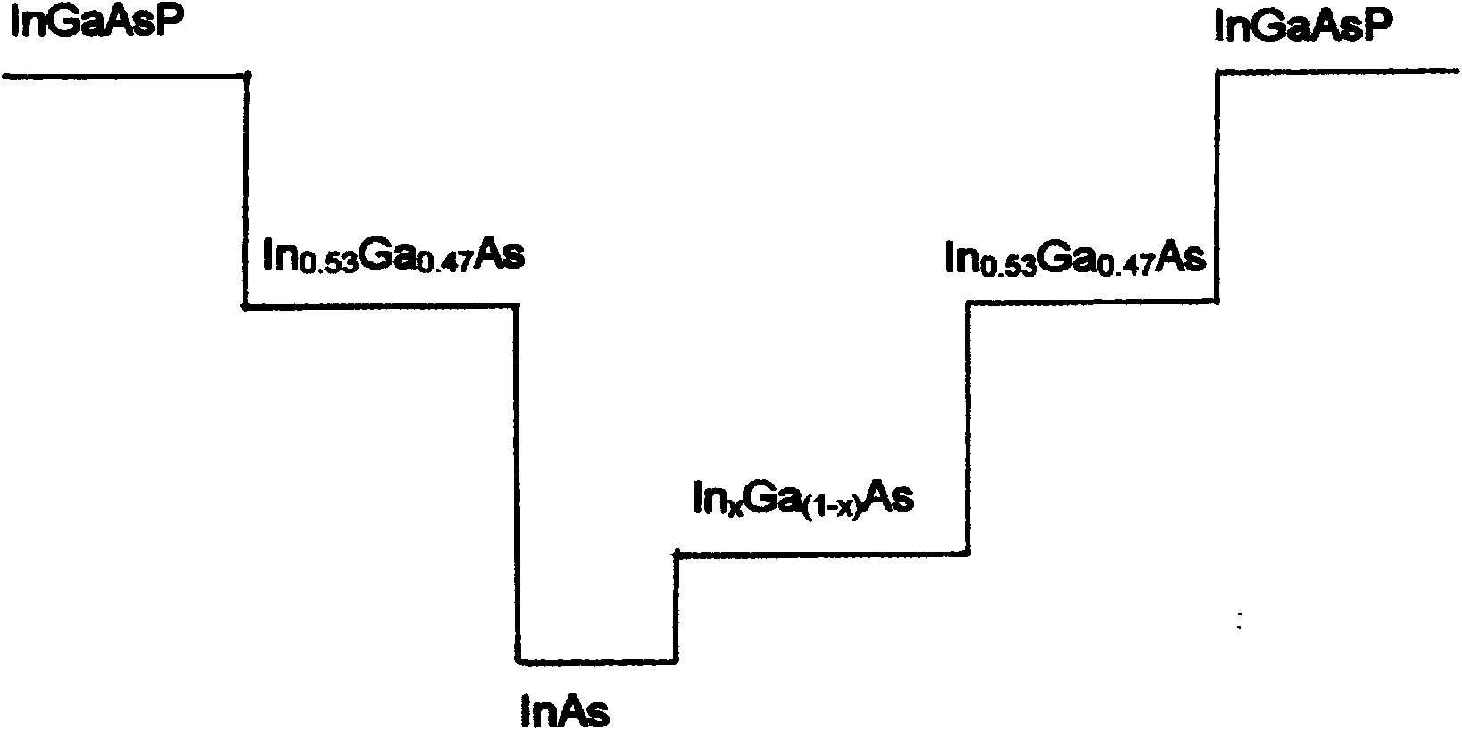
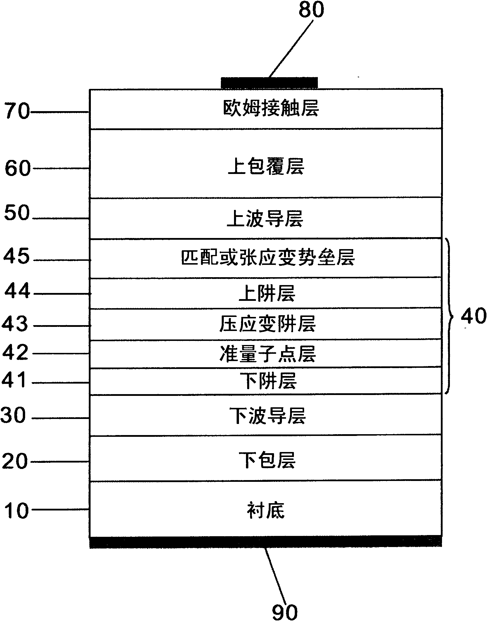
[0031] See figure 1 As shown, the present invention provides an InP-based long wavelength 2-3μm quasi-quantum dot laser structure, including:

[0032] A substrate 10, the substrate 10 is a heavily doped InP(001) substrate, the doping element is Si, and the doping concentration is (0.5-7)×10 18 / cm 3 ;

[0033] The lower cladding layer 20, which is made on the substrate 10, is an InP lower cladding layer, and its lattice constant matches the lattice constant of the substrate 10. The so-called lattice constant matching refers to the lattice constant of the epitaxial material and The lattice constant of InP(001) substrate is the same, and there is no stress between the two during epitaxial growth. The growth thickness of the lower cladding layer 20 is 0-3000nm, which is n-type doped, the doping element is Si, and the doping concentration is (0.1-5)×10 18 / cm 3 , It is doped to better provide electrons to the active area. The lower cladding layer 20 also functions as a buffer layer. At...


PUM

PropertyMeasurementUnit
Wavelengthaaaaaaaaaa
Growth thicknessaaaaaaaaaa

Abstract

The invention relates to an InP based long wavelength 2-3mum quasi-quantum dot laser structure. The laser structure comprises a substrate, a lower cladding, a lower waveguide layer, a matching or tensile strain structural layer with a period of 1-20, an upper waveguide layer, an upper cladding, an ohmic contact layer, an upper electrode and a lower electrode, wherein the lower cladding layer is manufactured on the substrate; the lower waveguide layer is manufactured on the lower cladding and used as a carrier limit layer for improving the electron-hole composite efficiency and the working temperature of the laser; the matching or tensile strain structural layer is manufactured on the lower waveguide layer and used as an active region of the laser and is a core part of the laser; the upper waveguide layer is manufactured on the matching or tensile strain structural layer with a period of 1-20 and used as a carrier limit layer for limiting carriers in the active region so as to increase the electron-hole composite efficiency and the working temperature of the laser; the upper cladding layer is manufactured on the upper waveguide layer; the ohmic contact layer is manufactured on the upper cladding, and the lattice constant of the ohmic contact layer is matched with that of the substrate; the upper electrode layer is manufactured on the ohmic contact layer and used for providing holes for the active region; and the lower electrode is manufactured on the thinned substrate and used for providing electrons for the active region.

Description

Technical field [0001] The present invention and semiconductor laser technology are mainly to grow InP for long-wavelength (2-3μm) quantum short-line laser on heavily doped InP(001) substrate. 0.53 Ga 0.47 As / InAs / In x Ga (1-x) As(0.58<x<0.83) / In 0.53 Ga 0.47 As / InGaAsP (matching or tensile strain) structure, especially refers to a multi-period In 0.53 Ga 0.47 As / InAs / In x Ga (1-x) As(0.58<x<0.83) / In 0.53 Ga 0.47 The As / InGaAsP (matched or tensile strain) quantum dot-step quantum well structure is a long-wavelength (2-3μm) InAs quasi-quantum dot laser structure in the active region. Background technique [0002] In recent years, lasers operating in the mid-infrared band (2-3μm) at room temperature have attracted widespread attention because the lasers in this band are very useful in atmospheric environment monitoring, free space laser communications, medicine, industrial production, molecular spectroscopy, etc. The application prospects are mainly due to two factors: o...

Claims


Application Information

Patent Timeline
IPC IPC(8): H01S5/343
Inventor 孔金霞徐波王占国
Owner INST OF SEMICONDUCTORS - CHINESE ACAD OF SCI
Why Eureka
Try Eureka