Pixel circuit structure of silicon-based organic light-emitting diode (OLED) display chip and drive method thereof

A technology for display chips and pixel circuits, applied in circuits, electrical components, electrical solid devices, etc., can solve problems such as inconsistent threshold voltage uniformity, immature manufacturing technology, and unstable threshold voltage

Inactive Publication Date: 2011-05-25
GUANGDONG SINODISPLAY TECH
View PDF4 Cites 6 Cited by
  • Summary
  • Abstract
  • Description
  • Claims
  • Application Information

AI Technical Summary

Problems solved by technology

The early active backplane used a-Si (amorphous silicon, amorphous silicon) TFT technology, but due to the low mobility of amorphous silicon and the instability of threshold voltage, it was not successful, and then it was transferred to LTPS (Low Temperature Poly-Silicon, low temperature polysilicon) TFT technology
Compared with amorphous silicon, the mobility of LTPS is much higher, but the threshold voltage still has the problem of inconsistency in uniformity, so certain circuit compensation must be carried out in the design of the pixel circuit. Most of the existing OLED displays currently use All are LTPS TFT backplane technology
In terms of mass production of large-size OLEDs, LTPS manufacturing technology is still immature, and there is no unified standard production line. To prepare LTPS TFT backplanes, it is necessary to invest a huge amount of money to build a dedicated production line.

Method used


Image

  • Pixel circuit structure of silicon-based organic light-emitting diode (OLED) display chip and drive method thereof
  • Pixel circuit structure of silicon-based organic light-emitting diode (OLED) display chip and drive method thereof
  • Pixel circuit structure of silicon-based organic light-emitting diode (OLED) display chip and drive method thereof

Examples


Embodiment Construction

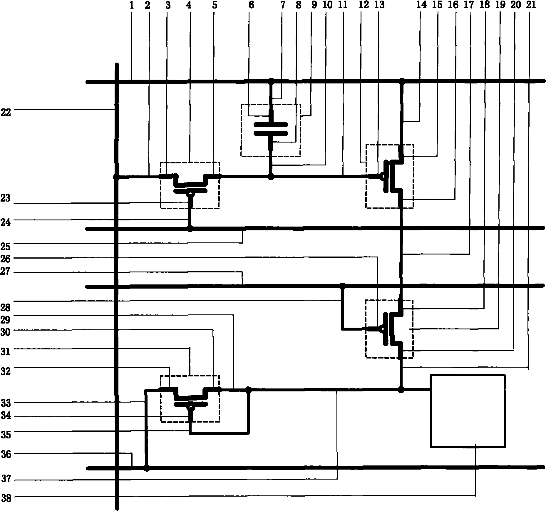
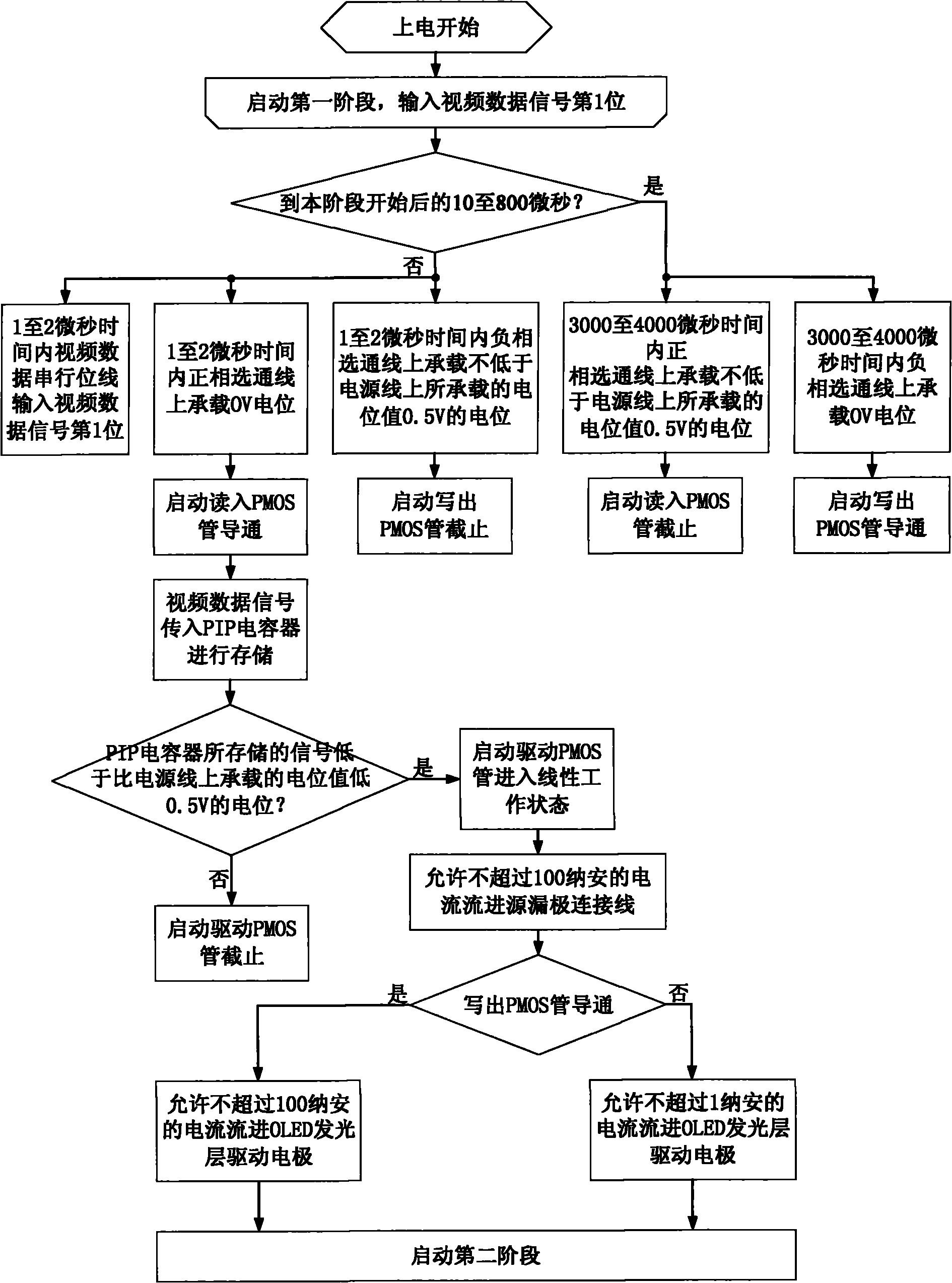
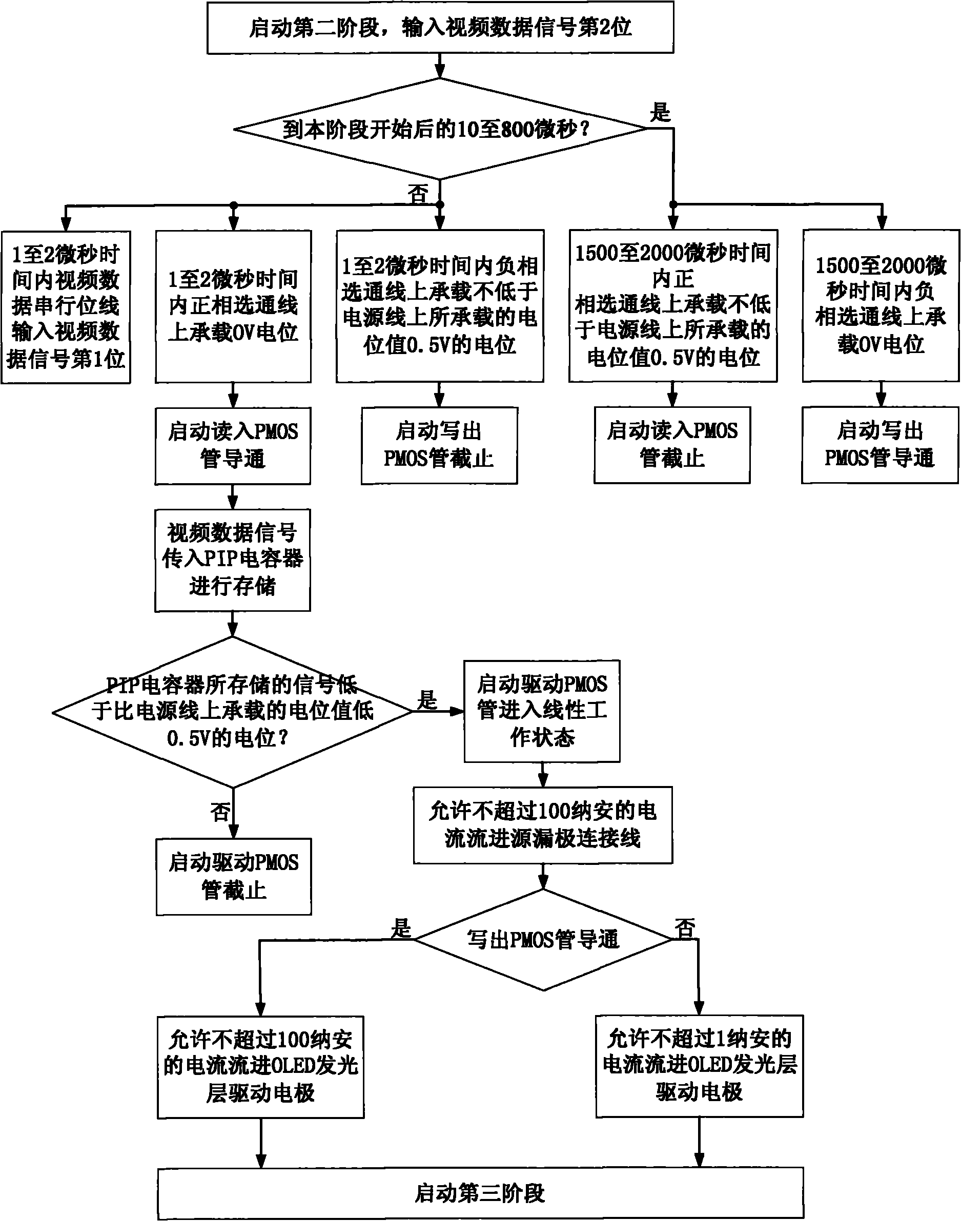
[0119] Attached below figure 1 The pixel circuit structure of a silicon-based OLED display chip of the present invention is further specifically described:

[0120]The silicon-based OLED display chip pixel circuit structure includes: a read-in PMOS transistor (4) composed of at least a read-in PMOS transistor source (3), a read-in PMOS transistor gate and a read-in PMOS transistor drain (5), A PIP capacitor (9) composed of at least a low-resistance polysilicon upper electrode (6) of a PIP capacitor and a high-resistance polysilicon lower electrode (8) of a PIP capacitor, at least a driving PMOS transistor source (15) and a driving PMOS transistor gate (13) And the driving PMOS transistor (12) formed by driving the drain of the PMOS transistor (16) is at least composed of the writing PMOS transistor source (18), the writing PMOS transistor grid (26) and the writing PMOS transistor drain (20) The writing PMOS transistor (19), the ground wire protection PMOS transistor composed ...


PUM


Abstract

The invention discloses a pixel circuit structure of a silicon-based OLED display chip and a drive method thereof. The pixel circuit structure at least has a reading-in p-channel metal oxide semiconductor (PMOS) pipe, a polysilicon-isolator-polysilicon (PIP) capacitor, a drive PMOS pipe, a writing-out PMOS pipe, a ground wire protection PMOS pipe, a video data serial bit line, a power wire which is connected with a PIP upper electrode connecting wire and a source connecting wire of the drive PMOS pipe at the same time, a 0V ground wire connected with a drain of the ground wire protection PMOS pipe through a drain connecting wire of the ground wire protection PMOS pipe, a positive phase row selection wire connected with a grid of the writing-in PMOS pipe through a grid connecting wire of the writing-in PMOS pipe, a negative phase row selection wire connected with the gird of the writing-out PMOS pipe through the grid connecting wire of the writing-out PMOS pipe, and an OLED luminescent layer drive electrode connected with a drive electrode connecting wire. The drive method comprises 9 steps which are carried out circularly after energization. The pixel circuit structure and the drive method thereof reduce production cost, the weight and space volume of the control drive circuit, and the power consumption of the whole machine.

Description

technical field [0001] The invention belongs to the technical field of microelectronics application in the discipline of information science and technology, and in particular relates to the field of a silicon-based OLED display chip pixel circuit structure and a driving method thereof. Background technique [0002] OLED (Organic Light Emitting Diode, Organic Light Emitting Diode) is a current-driven device, requiring the backplane circuit to provide accurate and stable current control. The early active backplane used a-Si (amorphous silicon, amorphous silicon) TFT technology, but due to the low mobility of amorphous silicon and the instability of threshold voltage, it was not successful, and then it was transferred to LTPS (Low Temperature Poly-Silicon, low temperature polysilicon) TFT technology. Compared with amorphous silicon, the mobility of LTPS is much higher, but the threshold voltage still has the problem of inconsistency in uniformity, so certain circuit compensati...

Claims


Application Information

Patent Timeline
Patent Type & Authority Applications(China)
IPC IPC(8): G09G3/32H01L27/32G09G3/3208
Inventor 郭海成代永平凌代年邱成峰彭华军黄飚
Owner GUANGDONG SINODISPLAY TECH
Why Eureka
Try Eureka