Blue light organic electroluminescence device

An electroluminescent device and electroluminescent technology, applied in the direction of electro-solid devices, electrical components, luminescent materials, etc., can solve the problems of OLED chromaticity, lack of stability, biased composite light-emitting area, etc., and achieve good chromaticity and long life. , the effect of high efficiency

Inactive Publication Date: 2011-06-01
KUNSHAN VISIONOX DISPLAY TECH +2
View PDF6 Cites 30 Cited by
  • Summary
  • Abstract
  • Description
  • Claims
  • Application Information

AI Technical Summary

Problems solved by technology
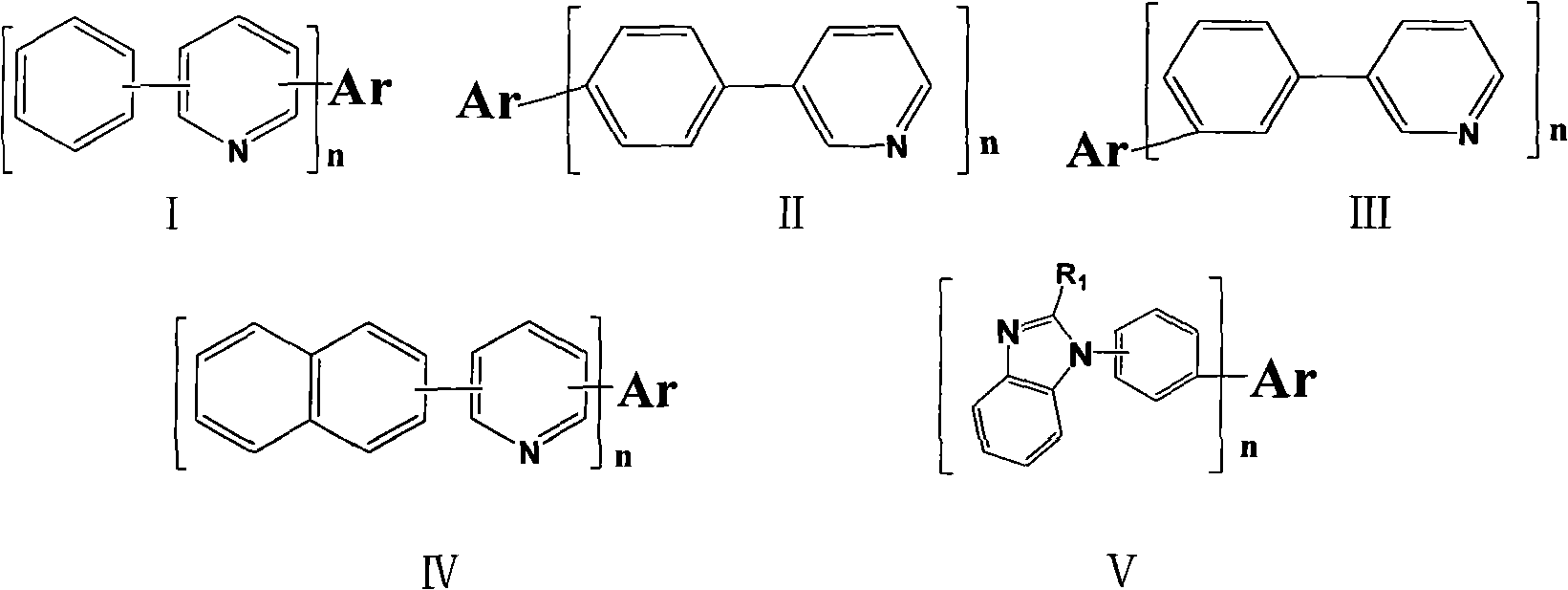
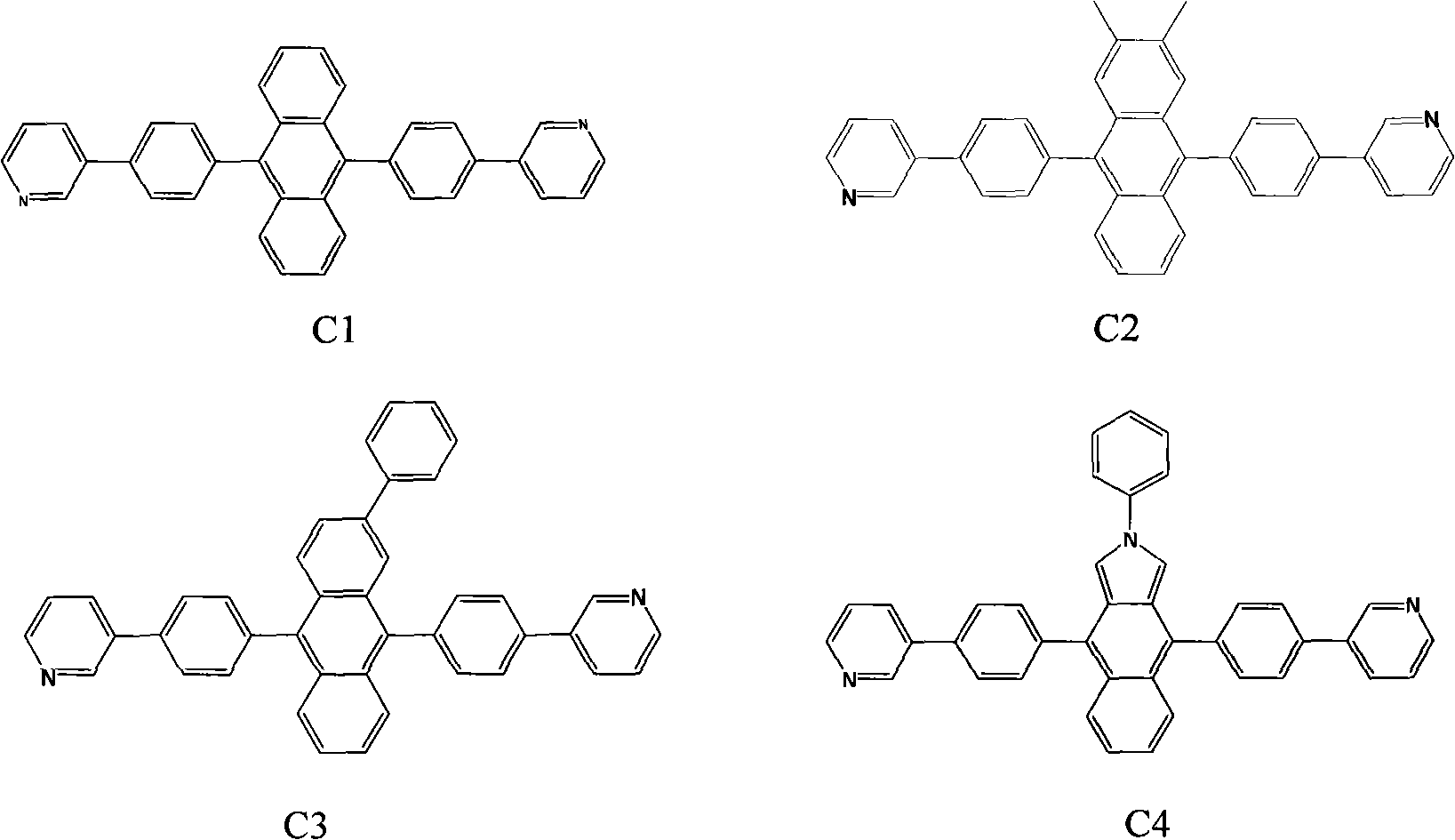
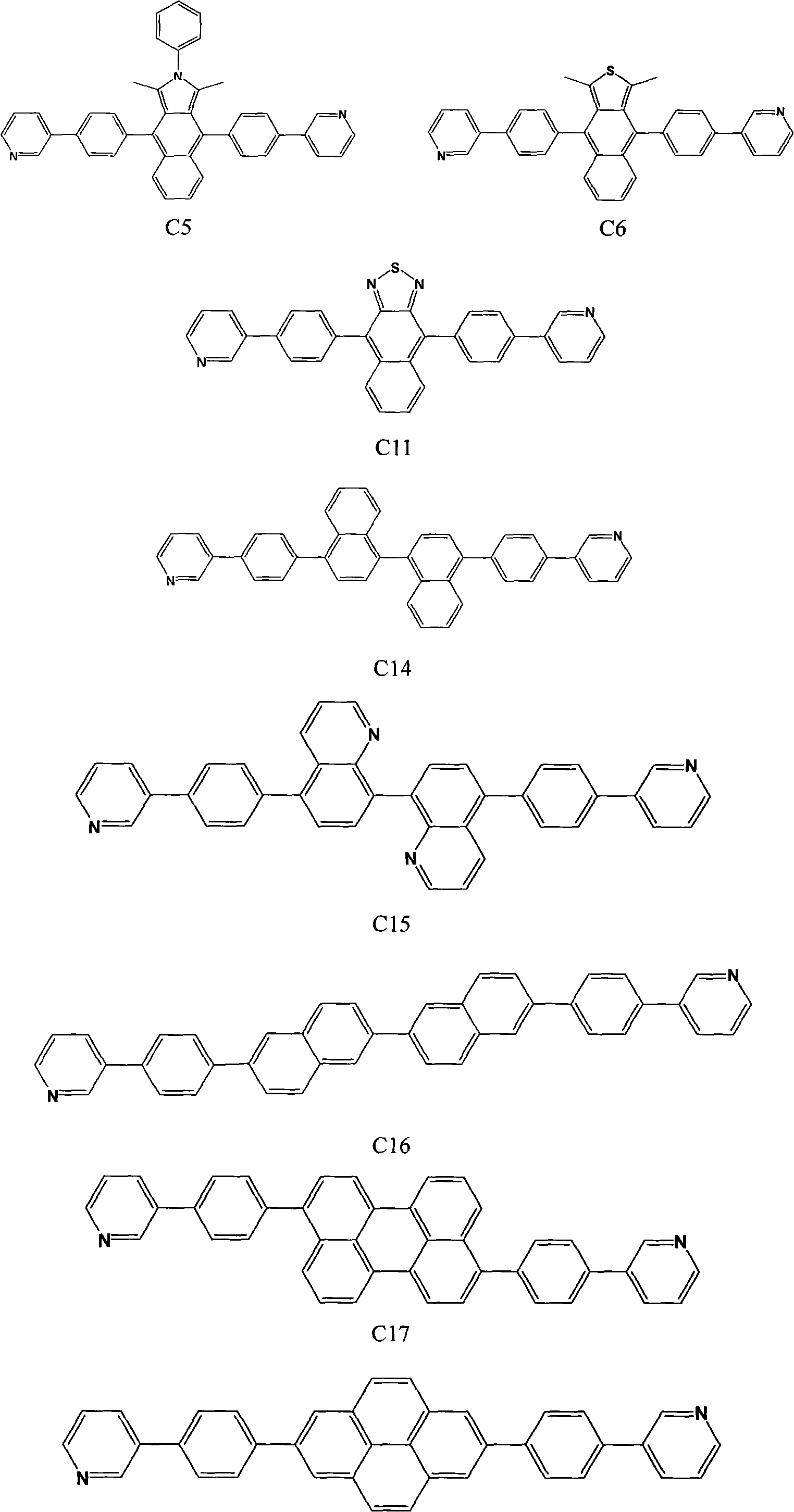
However, the electron transport ability of anthracene derivatives is stronger than the hole transport ability. When the ETL with high electron mobility is matched with the light-emitting host, it is easy to cause the composite light-emitting area to be biased towards the HTL interface, resulting in the lack of chromaticity and stability of OLEDs.

Method used


Image

  • Blue light organic electroluminescence device
  • Blue light organic electroluminescence device
  • Blue light organic electroluminescence device

Examples


Embodiment 1

[0056] Device structure: ITO / NPB(20nm) / NNPA: BD-2(30nm, 5%) / C25(20nm) / LiF(0.5nm) / Al(150nm)

[0057] With the ITO conductive glass substrate etched with specific patterns as the substrate, the substrate is ultrasonically cleaned in deionized water containing cleaning solution. The temperature of the cleaning solution is about 60°C, and then the cleaned substrate is cleaned Dry it, put it into the evaporation chamber to evaporate the hole injection layer, the hole transport layer, the light emitting layer, the electron transport layer, the electron injection layer, and the cathode structure in sequence, and the chamber pressure during the evaporation process is lower than 5.0×10 -3 pa.

[0058] In this embodiment, 20 nm of NPB is deposited on the surface of the ITO anode as a hole transport layer. The light-emitting layer is BD-2 doped with 5% of blue light host 9-(2-naphthyl)-10-[3-(2-naphthyl)phenyl]anthracene (NNPA), and the thickness of the light-emitting layer is 30nm. De...

Embodiment 2

[0060] Device structure: ITO / NPB(20nm) / NNPA: BD-5(40nm, 5%) / C11(10nm) / LiF(0.5nm) / Al(150nm)

[0061] The device with the above structure was prepared according to the method of Example 1, except that the thickness of the light-emitting layer was 40 nm, BD-5 was used as the luminescent dye, and C11 was used as the electron transport material, with a thickness of 10 nm.

Embodiment 3

[0063] Device structure: ITO / NPB(20nm) / PADN: BD-9(30nm, 1%) / C76(20nm) / LiF(0.5nm) / Al(150nm)

[0064] The device with the above structure was prepared according to the method of Example 1, except that 2-phenyl-9,10-bis(2-naphthyl)anthracene (PADN) was used as the main body of the light-emitting layer, BD-9 was a luminescent dye, and the doping ratio was 1%, the electron transport material is C76.


PUM

PropertyMeasurementUnit
porosityaaaaaaaaaa
thicknessaaaaaaaaaa
thicknessaaaaaaaaaa

Abstract

The invention discloses a blue light organic electroluminescence device. The device comprises a pair of electrodes and an organic luminous medium layer arranged between the electrodes, wherein the organic luminous medium layer at least comprises a luminous layer and an electron transmission layer, the luminous layer comprises a host material and a guest material, the hole mobility of the guest material is 10<-3>--10<-6>cm<2>V<-1>s<-1>, and the hole mobility of the guest material is 1 to 3 magnitude orders greater than electron mobility; the electron mobility of the electron transmission material is more than or equal to 10<-4>cm<2>V<-1>s<-1>; and the energy gap (Eg) of the guest material is 2.82-2.53eV. The organic electroluminescence device has the advantages of high efficiency, good chromaticity and long service life.

Description

technical field [0001] The present invention relates to an organic electroluminescence (EL) element, more specifically, relates to a high-efficiency organic EL element. technical background [0002] Organic electroluminescent display (hereinafter referred to as OLED) has a series of advantages such as self-luminescence, low-voltage DC drive, full curing, wide viewing angle, light weight, simple composition and process, etc. Compared with liquid crystal display, organic electroluminescent display is not It requires a backlight source, has a large viewing angle and low power, and its response speed can reach 1000 times that of a liquid crystal display, but its manufacturing cost is lower than that of a liquid crystal display with the same resolution. Therefore, organic electroluminescent displays have broad application prospects. [0003] The general structure of an organic electroluminescent device includes in turn: a substrate, an anode, an organic layer, and a cathode, and ...

Claims


Application Information

Patent Timeline
Patent Type & Authority Applications(China)
IPC IPC(8): H01L51/50H01L51/54C09K11/06
CPCC09B57/00C09B57/001C09B1/00C09B3/14
Inventor 邱勇谢静董艳波
Owner KUNSHAN VISIONOX DISPLAY TECH
Why Eureka
Try Eureka