

Method for implementing base region window of silicon germanium heterojunction transistor
A heterojunction transistor and base technology, applied in semiconductor devices, semiconductor/solid-state device manufacturing, electrical components, etc., can solve the problems of discontinuous metal silicide, increased resistance of the outer base, and insufficient insulation. Achieve the effect of eliminating sidewall residues, reducing base resistance, and reducing defects
- Summary
- Abstract
- Description
- Claims
- Application Information
AI Technical Summary
Problems solved by technology
Method used
Image

Examples
Embodiment Construction
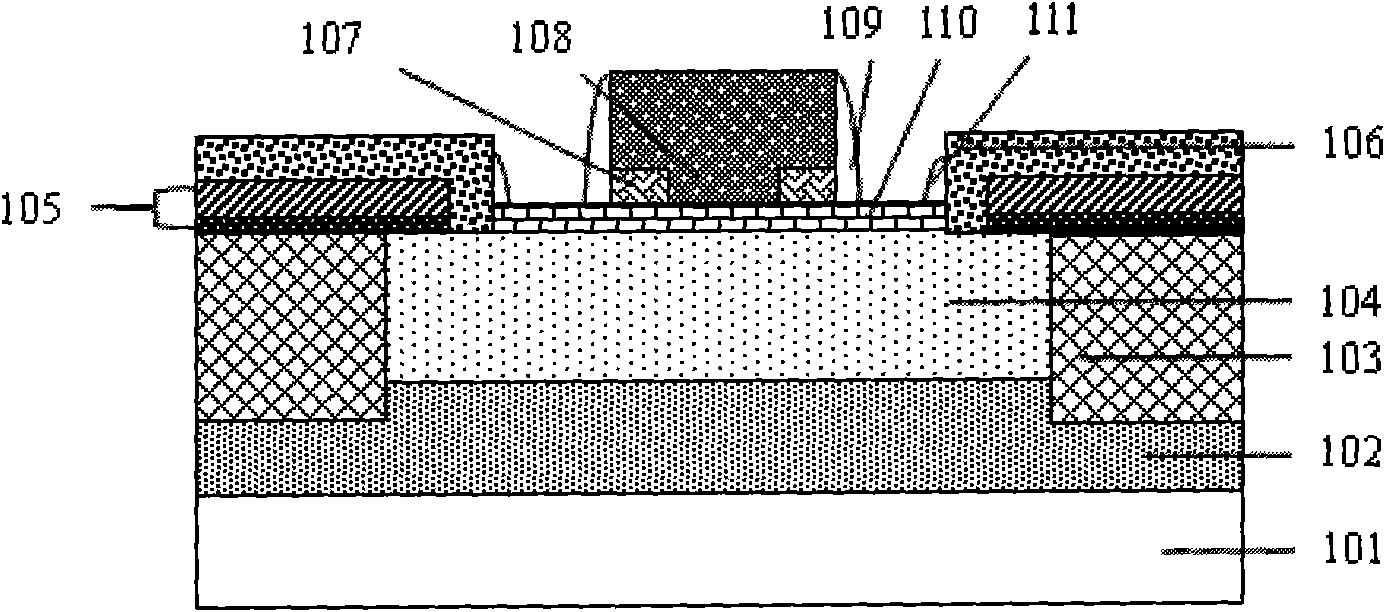
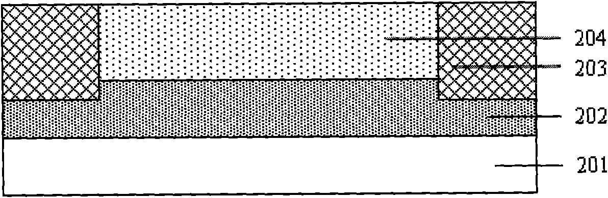
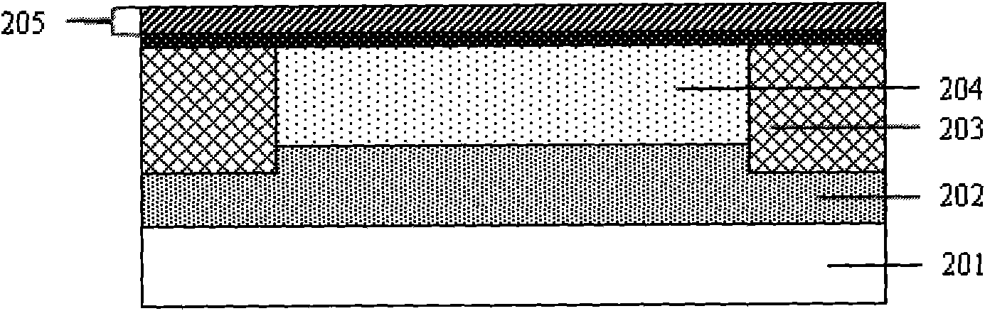
[0020] The method for realizing the base region window of the silicon-germanium heterojunction transistor described in the present invention is to deposit a layer of dielectric film layer after the dielectric film is partially opened and before the oxide film is removed, and use the dielectric film layer to form a step in the base region window interface. A D-shaped side wall is formed; at the same time, using the protection of the D-shaped side wall, the remaining oxide film in the window of the base region is removed by wet method, and the SiGe base region is epitaxially grown in a short time. The formation of the D-shaped sidewall makes the step of the window interface of the base area gradually changed. After SiGe epitaxy, the gradually changed step formed by the D-shaped sidewall remains, so that there is no insulator residue in the subsequent emitter polysilicon sidewall process. In this way, a continuous metal silicide is formed to reduce the resistance of the outer base...
PUM
 Abstract
Description
Claims
Application Information