Forming method of dual-damascene structure

A dual damascene structure and patterning technology, which is applied in the manufacture of electrical components, semiconductor/solid-state devices, circuits, etc., can solve the problems affecting the margin of the manufacturing process, the dual damascene structure, the difficulty of filling the anti-reflection layer through holes, etc., and achieve the goal of optimizing the gap Groove etching effect, improved critical dimension accuracy, easy to form and etch effect

Inactive Publication Date: 2011-06-15
SEMICON MFG INT (SHANGHAI) CORP +1
View PDF5 Cites 6 Cited by
  • Summary
  • Abstract
  • Description
  • Claims
  • Application Information

AI Technical Summary

Problems solved by technology

[0012] As the critical dimension of the existing dual damascene structure becomes smaller and smaller, the minimum resolution of the photolithography process is continuously improved, and the depth of field is also smaller and smaller, so that the flattening degree of the exposure surface is required to be higher and higher; at the same time, the smaller The through-hole size of the anti-reflection layer also makes the through-hole filling of the anti-reflection layer more and more difficult. Therefore, the effect of the through-hole filling process of the anti-reflection layer will greatly affect the margin of the entire manufacturing process and the quality of the dual damascene structure.

Method used


Image

  • Forming method of dual-damascene structure
  • Forming method of dual-damascene structure
  • Forming method of dual-damascene structure

Examples


Embodiment Construction

[0031] In the actual manufacture of the dual damascene structure, the prior art method will cause uneven distribution of the line width of the exposure pattern during the trench photolithography process, resulting in inaccurate critical dimensions of the dual damascene structure. After research, it was found that the problem was caused by photolithography defocus and shallow depth of focus.

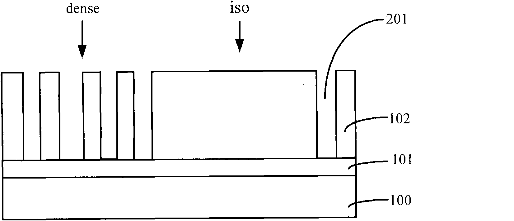
[0032] Further, the inventors found that because there are more through holes in the dense area, in the third step, that is, in the through hole filling process, voids occur after filling the through holes, such as Figure 7 As shown, the height a of dense area dense after filling is smaller than the height b of isolated area iso. The maximum difference dense / iso bias between the dense area and the isolated area is defined as the maximum height b of the isolated area minus the minimum height a of the dense area, the formula is as follows:

[0033] dense / iso bias=Max(iso)-Min(dense)=b-a ...


PUM


Abstract

The invention relates to a forming method of a dual-damascene structure, comprising the following steps of: providing a substrate, wherein the surface of the substrate is provided with conductive areas, an inter-layer dielectric layer is formed on the substrate, through holes are formed in the inter-layer dielectric layer, and the positions of the through holes correspond to the positions of the conductive areas; forming a first anti-reflection layer on the inter-layer dielectric layer and in the through holes, and filling the contact through holes; forming a second anti-reflection layer on the first anti-reflection layer, wherein the viscosity of the second anti-reflection layer is larger than that of the first anti-reflection layer; carrying out groove imaging on the second anti-reflection layer, the first anti-reflection layer and the inter-layer dielectric layer, etching the second anti-reflection layer, the first anti-reflection and partial inter-layer dielectric layer to form a groove, wherein the bottom of the groove is communicated with at least one through hole; filling a conducting material in the groove and the through holes; and flattening the conducting material to form the dual-damascene structure.

Description

technical field [0001] The invention relates to a semiconductor manufacturing process, in particular to a method for forming a double damascene structure. Background technique [0002] With the development of semiconductor devices, semiconductor devices already have a deep submicron structure, and a semiconductor integrated circuit (IC) contains a huge number of semiconductor elements. In this large-scale integrated circuit, not only a single-layer interconnection structure is included, but also interconnection between multiple layers is included. Therefore, a multi-layer interconnection structure is also included, in which multiple interconnection layers are stacked on top of each other, and are connected through Interlayer dielectric layers between multiple interconnection layers provide isolation. In particular, when using a dual-damascene process to form a multi-layer interconnection structure, it is necessary to form trenches and via holes for interconnection in the in...

Claims


Application Information

Patent Timeline
Patent Type & Authority Applications(China)
IPC IPC(8): H01L21/768
Inventor 田彬安辉
Owner SEMICON MFG INT (SHANGHAI) CORP
Why Eureka
Try Eureka