Method for detecting pinhole type growth defect

A pinhole and defect technology, which is applied in the detection field of semiconductor pinhole growth defects, can solve problems such as burning defects, waste of production costs, and no help

Inactive Publication Date: 2011-06-29
SEMICON MFG INT (SHANGHAI) CORP
View PDF0 Cites 18 Cited by
  • Summary
  • Abstract
  • Description
  • Claims
  • Application Information

AI Technical Summary

Problems solved by technology

[0005] However, due to the method of electrical testing, a large current will be generated at the defect, and the heat released by the thermal effect of the current will destroy or even burn the original appearance of the defect. Therefore, TEM can only see the gate at the defect, and the gate oxide layer The phenomenon of fusion with the active area and the observation of the defect morphology whose original appearance is destroyed are not helpful for judging whether there are pinhole growth defects in Gate Oxide itself and the analysis of the cause of the defects.
Moreover, the subsequent manufacturing process will also affect the performance of Gate Oxide, so it is impossible to determine whether the electrical test defects are pinhole growth defects of Gate Oxide itself.
In addition, it is also a great waste of production cost to find Gate Oxide failure through the electrical test at the WAT stage

Method used


Image

  • Method for detecting pinhole type growth defect
  • Method for detecting pinhole type growth defect
  • Method for detecting pinhole type growth defect

Examples


Embodiment Construction

[0026] In order to make the purpose, technical solution, and advantages of the present invention clearer, the present invention will be further described in detail below with reference to the accompanying drawings and examples.

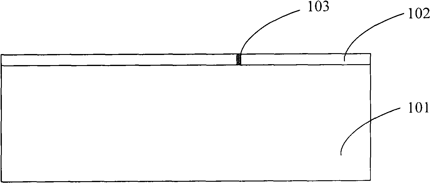
[0027] In the manufacturing process of semiconductor MOSFET devices, in order to detect the growth of MOSFET devices, a semiconductor silicon substrate is placed as a control piece at the same time, and the grown control piece is used as a sample for failure analysis to reflect the performance of the actually grown MOSFET device. The specific steps of the detection method for pinhole growth defects on the oxide layer of the chip gate are as follows:

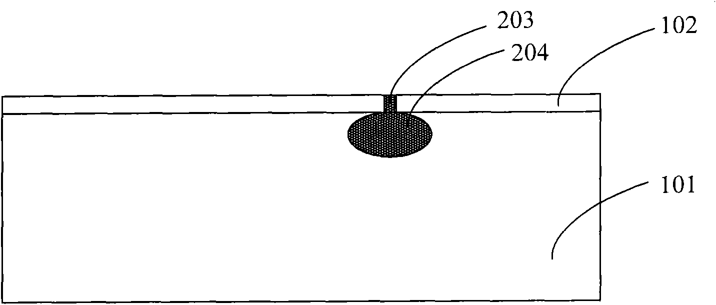
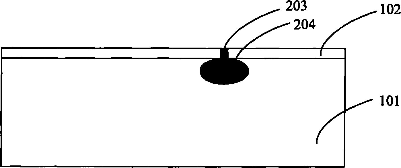
[0028] Step 1, growing a silicon dioxide gate oxide layer 102 on the semiconductor silicon substrate 101, such as figure 1 As shown, there are pinhole growth defects 103 on the gate oxide layer 102;

[0029] In this step, the method for growing the silicon dioxide gate oxide layer 102 is furnace tube gr...


PUM


Abstract

The invention provides a method for detecting a pinhole type growth defect. The method comprises the following steps of: growing a silicon dioxide gate oxide layer on a semiconductor silicon substrate; corroding the gate oxide layer by using mixed solution of nitric acid, hydrofluoric acid and water; forming a hole on the semiconductor silicon substrate below the pinhole type growth defect of the gate oxide layer; flushing the surface of the gate oxide layer by using deionized water, then detecting the hole through an optical microscope and determining the position of the pinhole type growth defect of the gate oxide layer; and finally preparing a sample at the position of the pinhole type growth defect and accurately detecting the position of the pinhole type growth defect. By the method, the pinhole type growth defect of the gate oxide layer can be detected in real time, the sample can be quickly and accurately prepared at the position of the pinhole type growth defect, and the position of the pinhole type growth defect can be precisely detected by a transmission electron microscope.

Description

technical field [0001] The invention relates to a detection method for semiconductor pinhole growth defects, in particular to a detection method for pinhole growth defects. Background technique [0002] The Metal-Oxide Semiconductor Field Effect Transistor (MOSFET) device structure includes an active region in the semiconductor silicon substrate, a gate (Gate poly) above the active region, and active gates on both sides of the gate. The regions are the source and drain formed by ion implantation, the conductive channel under the gate, and the gate oxide layer (GateOxide) between the gate and the conductive channel. In the manufacturing process of MOSFET, the gate oxide layer and the gate are first grown on the semiconductor silicon substrate, and then other structures of the MOSFET device are grown. Among them, the pinhole growth defects of Gate Oxide will directly lead to the failure of Gate Oxide performance test. In the manufacturing process of a semiconductor device, in...

Claims


Application Information

Patent Timeline
Patent Type & Authority Applications(China)
IPC IPC(8): H01L21/66H01L21/306
Inventor 任正鹏
Owner SEMICON MFG INT (SHANGHAI) CORP
Why Eureka
Try Eureka