
Two-dimensional photonic crystal four-wavelength division multiplexer based on multiple-mode interference

A two-dimensional photonic crystal and wavelength division multiplexer technology, applied in the directions of light guides, optics, instruments, etc., can solve the problems of unsatisfactory insertion loss and optical isolation performance parameters, high optical isolation, small insertion loss, etc. Compact, easy to integrate, and the effect of reducing insertion loss

Inactive Publication Date: 2011-07-06
NANJING UNIV OF POSTS & TELECOMM
View PDF1 Cites 18 Cited by
  • Summary
  • Abstract
  • Description
  • Claims
  • Application Information

AI Technical Summary

Problems solved by technology

[0007] Technical solution: In order to adapt to the rapid growth of network data and the development trend of miniaturization and integration of communication devices, and to overcome the shortcomings of using traditional optical fiber waveguides to make wavelength division multiplexing devices with large volume and unsatisfactory performance parameters of insertion loss and optical isolation, this The invention proposes a two-dimensional photonic crystal four-wavelength wavelength division multiplexer based on multi-mode interference, which uses the photonic band gap of photonic crystals to filter light, and has the characteristics of small size and easy integration. Based on multi-mode interference The self-imaging feature realizes the demultiplexing function, has small insertion loss and high optical isolation, and is suitable for the development of future miniaturized optical communication devices.

Method used


Image

  • Two-dimensional photonic crystal four-wavelength division multiplexer based on multiple-mode interference
  • Two-dimensional photonic crystal four-wavelength division multiplexer based on multiple-mode interference
  • Two-dimensional photonic crystal four-wavelength division multiplexer based on multiple-mode interference

Examples


Embodiment Construction

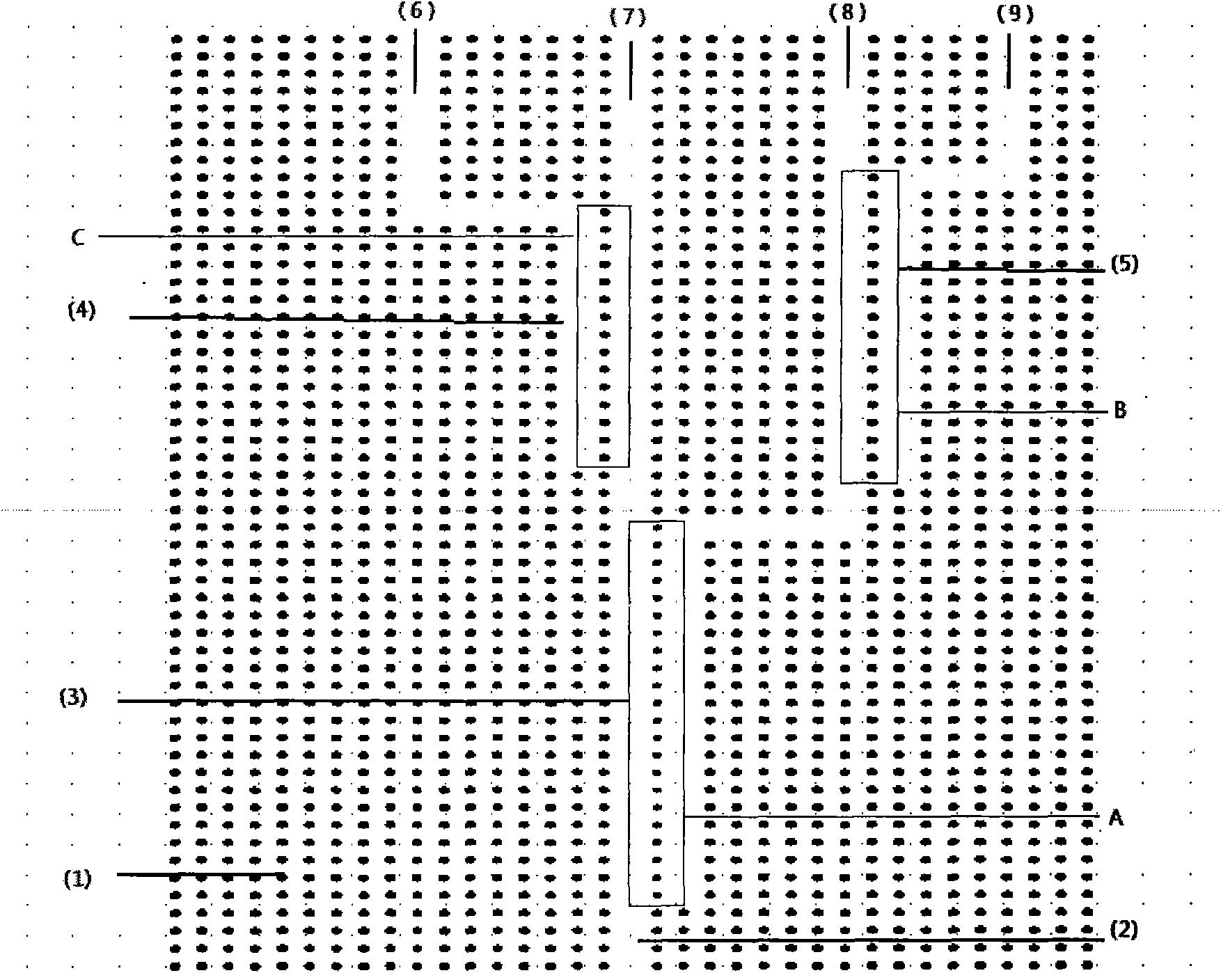
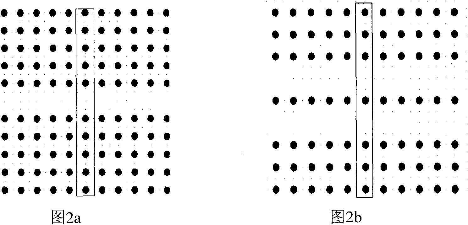
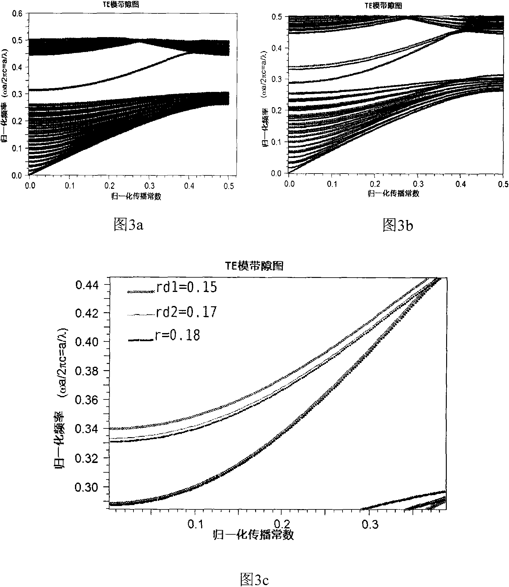
[0017] The two-dimensional photonic crystal four-wavelength wavelength division multiplexer based on the multimode interference theory of the present invention mainly includes a two-dimensional periodic arrangement of dielectric column photonic crystals, a single-mode input waveguide, a multimode interference coupling region, and a single-mode output waveguide; the wavelengths are different The four light waves pass through the single-mode input waveguide and pass through the multi-mode interference coupling region. Since the light waves of different wavelengths have different coupling beat lengths, images at different positions are formed, and then the four light waves of different wavelengths are respectively output by the single-mode output waveguide.

[0018] The two-dimensional periodic dielectric pillar photonic crystal is a dielectric pillar GaAs photonic crystal with a square periodic distribution along the X-Z plane. The single-mode waveguide is obtained by removing a r...


PUM


Abstract

The invention relates to a two-dimensional photonic crystal four-wavelength division multiplexer based on multiple-mode interference, which comprises two-dimensional periodically arrayed medium column photonic crystals (1), wherein the multiplexer also comprises a single mode input waveguide (2), a first multi-mode interference coupling area (3), a second multi-mode interference coupling area (4), a third multi-mode interference coupling area (5), a first single mode output waveguide (6), a second single mode output waveguide (7), a third single mode output waveguide (8) and a fourth single mode output waveguide (9), which are arranged between the medium column photonic crystals (1). By finely tuning the size of the radius of the medium column in the coupling area, the structure of component is more compact and the property parameter is more optimized.

Description

technical field [0001] The invention provides a two-dimensional photonic crystal four-wavelength wavelength division multiplexer based on multi-mode interference and a design method thereof, and relates to the technical field of photonic crystals and optical communication. Background technique [0002] At present, due to the rapid growth of network data and the development trend of miniaturization and integration of communication devices, it is urgent to use new miniaturized photonic crystal devices to expand network capacity. The main technologies to expand the capacity of optical fibers include electrical time division multiplexing, optical time division multiplexing, wavelength division multiplexing and optical solitons. Wavelength division multiplexing technology can expand the capacity of optical fiber communication without laying new optical fiber lines, the network upgrade is convenient, and the existing electrical network can be superimposed on the optical network. I...

Claims


Application Information

Patent Timeline
Patent Type & Authority Applications(China)
IPC IPC(8): G02B6/293G02B6/122
Inventor 陈鹤鸣金晓君
Owner NANJING UNIV OF POSTS & TELECOMM
Learn More