Method for manufacturing silicon oxynitride gate oxide layer

A silicon oxynitride gate and silicon oxynitride technology, which is applied in semiconductor/solid-state device manufacturing, electrical components, semiconductor devices, etc., can solve problems affecting device reliability, device threshold voltage instability, etc. Effect of Density Reduction and Reliability Improvement

Active Publication Date: 2013-03-13
SEMICON MFG INT (SHANGHAI) CORP +1
View PDF0 Cites 1 Cited by
  • Summary
  • Abstract
  • Description
  • Claims
  • Application Information

AI Technical Summary

Problems solved by technology

With the increase of the charge and discharge times of the gate capacitance, the threshold voltage of the device will eventually become unstable, which will affect the reliability of the device.

Method used


Image

  • Method for manufacturing silicon oxynitride gate oxide layer
  • Method for manufacturing silicon oxynitride gate oxide layer
  • Method for manufacturing silicon oxynitride gate oxide layer

Examples


Embodiment Construction

[0037] In order to make the object, technical solution, and advantages of the present invention clearer, the present invention will be further described in detail below with reference to the accompanying drawings and examples.

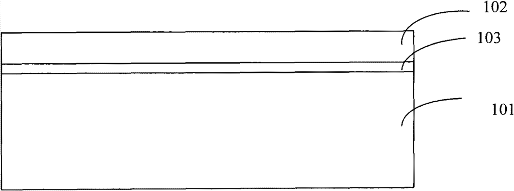
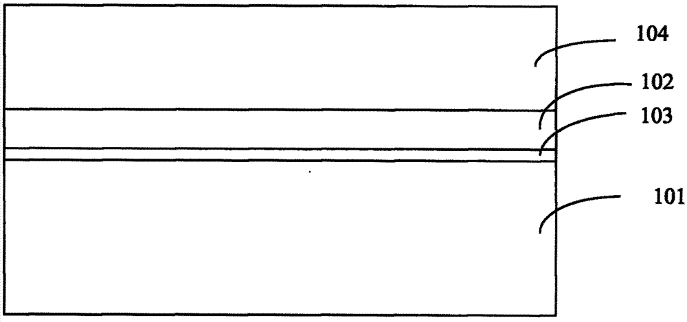
[0038] combine Figure 5 ~ Figure 8 The schematic cross-sectional structure diagram of the fabrication of the silicon oxynitride gate oxide layer of the present invention illustrates the fabrication steps of the silicon oxynitride gate oxide layer of the present invention.

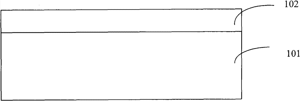
[0039] Step one, see Figure 5 , providing a silicon substrate 101, simultaneously nitriding the silicon substrate 101, and forming silicon oxynitride 202 on the silicon substrate;

[0040] In this step, the method for forming silicon oxynitride on a silicon nitride substrate is to feed nitrous oxide (N 2 O), or reaction gases containing nitrogen and oxygen such as nitric oxide (NO), the present embodiment uses nitric oxide gas. Nitrogen can also be used as an auxiliary gas whil...


PUM

PropertyMeasurementUnit
thicknessaaaaaaaaaa

Abstract

The invention provides a method for manufacturing a silicon oxynitride gate oxide layer of an MOS (metal oxide semiconductor) device, and the method comprises the following steps: firstly nitridizing on a provided silicon substrate for forming silicon oxynitride, then performing thermal oxidization for forming a first silicon oxide layer between the silicon oxynitride and the silicon substrate and a second silicon oxide layer on the silicon oxynitride, and then depositing polysilicon on the second silicon oxide layer after secondly annealing the silicon substrate; and etching for forming a gate and the silicon oxynitride gate oxide layer. The silicon oxide layer is introduced between the silicon substrate and the silicon oxynitride, thereby reducing dangling bonds between the silicon oxynitride gate oxide layer and the silicon substrate, further reducing the interface state charge density between the silicon oxynitride gate oxide layer and the substrate and improving certain properties of the MOS device, such as improving the stability of threshold voltage of the device, reducing the hot-carrier effect and the flicker noise of the device and the like.

Description

technical field [0001] The invention relates to the field of semiconductor manufacturing, in particular to a method for manufacturing a silicon oxynitride gate oxide layer. Background technique [0002] A Metal-Oxide Semiconductor Field Effect Transistor (MOS) device structure includes an active region, a source, a drain and a gate, wherein the active region is located in a semiconductor silicon substrate, and the gate The electrode is located above the active region, and the active regions on both sides of the gate are respectively implanted with ions to form a source and a drain. There is a conductive channel under the gate, and there is a gate oxide between the gate and the conductive channel. layer. According to different types of ion implantation, MOS devices are divided into PMOS devices and NMOS devices. In the manufacturing process of the MOS device, the gate oxide layer and the gate are first grown on the semiconductor silicon substrate, and then other structures ...

Claims


Application Information

Patent Timeline
Patent Type & Authority Patents(China)
IPC IPC(8): H01L21/28H01L21/336
Inventor 高伟辉陆肇勇
Owner SEMICON MFG INT (SHANGHAI) CORP
Why Eureka
Try Eureka