Groove-interconnected wafer level MOSFET encapsulation structure and implementation method

A technology of packaging structure and implementation method, which is applied in electrical components, electrical solid devices, circuits, etc., to achieve the effects of low packaging cost, shortened interconnection distance, and improved current carrying capacity

Active Publication Date: 2012-07-25
JIANGYIN CHANGDIAN ADVANCED PACKAGING CO LTD
View PDF0 Cites 0 Cited by
  • Summary
  • Abstract
  • Description
  • Claims
  • Application Information

AI Technical Summary

Problems solved by technology

[0005] The purpose of the present invention is to overcome the deficiencies of the traditional MOSFET packaging structure and its implementation method, to provide a high-performance trench interconnection wafer-level MOSFET packaging structure and a realization method with high production efficiency and low packaging cost

Method used


Image

  • Groove-interconnected wafer level MOSFET encapsulation structure and implementation method
  • Groove-interconnected wafer level MOSFET encapsulation structure and implementation method
  • Groove-interconnected wafer level MOSFET encapsulation structure and implementation method

Examples


Embodiment Construction

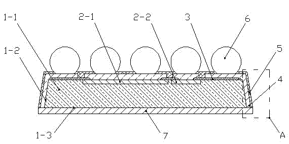
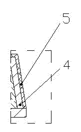
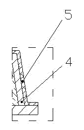
[0023] see figure 1 , figure 1 It is a cross-section schematic diagram of the packaging structure of the trench-interconnected wafer-level MOSFET of the present invention. Depend on figure 1 It can be seen that the trench interconnection wafer-level MOSFET packaging structure of the present invention includes a chip body 1-1, a chip trench 1-2, a chip source electrode 2-1, a chip gate electrode 2-2, and a chip surface protection layer 3 , circuit layer 4, circuit surface protective layer 5, solder ball 6 and back metal layer 7, the chip source electrode 2-1 and chip gate electrode 2-2 are arranged on the front of the chip body 1-1, and the chip surface protective layer 3 is arranged On the front of the chip body 1-1, the chip source electrode 2-1 and the chip gate electrode 2-2, the chip groove 1-2 runs through the front and back of the chip body 1-1, and the circuit layer 4 is arranged on the chip source electrode 2-1. The surface of the chip gate electrode 2-2 and the chi...


PUM


Abstract

The invention relates to a groove-interconnected wafer level metal-oxide-semiconductor field effect transistor (MOSFET) encapsulation structure and an implementation method. The structure comprises a chip body (1-1); a chip source electrode (2-1) and a chip gate electrode (2-2) are arranged on the front surface of the chip body; chip surface protection layers (3) are arranged on the front surfaces of the chip source electrode and the chip gate electrode of the chip body; chip grooves (1-2) pass through the front surface and the back surface of the chip body; circuit layers (4) are arranged onthe surface of the chip source electrode, the surface of the chip gate electrode and the surfaces of the chip surface protection layers (3) and in the chip grooves (1-2); a circuit surface protectionlayer (5) is arranged on the surface of the circuit layer; welded balls (6) are arranged on the surfaces of the circuit layers (4) on the front surface of the chip body (1-1); a back surface metal layer (7) is arranged on the back surface (1-3) of the chip body (1-1); and the back surface metal layer (7) is interconnected with the circuit layers (4). The encapsulation structure with high performance, and a process method which is used for implementing the structure and has high production efficiency and is low in encapsulation cost are provided.

Description

technical field [0001] The invention relates to a wafer level chip size packaging structure and a realization method. It belongs to the technical field of semiconductor packaging. Background technique [0002] MOSFET (Metal Oxide Semiconductor Field Effect Transistor) is a field effect transistor that uses electric field effects to control semiconductors. MOSFETs have received increasing attention in recent years due to their characteristic of enabling low power consumption voltage control. The performance of MOSFET, especially the current carrying capacity, largely depends on the heat dissipation performance, and the heat dissipation performance mainly depends on the package form. However, traditional MOSFET packages are mainly in the form of TO, SOT, SOP, QFN, QFP, etc. This type of package wraps the chip in a plastic package, which cannot conduct or dissipate the heat generated by the chip in time, which restricts the performance improvement of the MSOFET. . Moreover,...

Claims


Application Information

Patent Timeline
Patent Type & Authority Patents(China)
IPC IPC(8): H01L29/78H01L29/417H01L23/367H01L21/50
CPCH01L2224/13H01L2924/13091
Inventor 陈栋张黎陈锦辉赖志明
Owner JIANGYIN CHANGDIAN ADVANCED PACKAGING CO LTD
Why Eureka
Try Eureka