Floating gates of EEPROM (electrically erasable programmable read-only memory) and manufacturing method thereof

A manufacturing method and floating gate technology, applied in semiconductor/solid-state device manufacturing, electrical components, semiconductor devices, etc., can solve the problems of affecting the effect of blocking electrons, uneven film thickness, etc., and achieve the effect of improving data retention characteristics

Active Publication Date: 2011-07-20
SHANGHAI HUAHONG GRACE SEMICON MFG CORP
View PDF0 Cites 8 Cited by
  • Summary
  • Abstract
  • Description
  • Claims
  • Application Information

AI Technical Summary

Problems solved by technology

When the floating gate 12 has a vertical etching profile, it is easy to form an acute angle on the upper corner of the floating gate 12, which will cause the bottom silicon oxide of the ONO layer 13 to have an uneven film thickness at the edge of the floating gate 12, thereby affecting the ONO layer 13. The effect of blocking electrons

Method used


Image

  • Floating gates of EEPROM (electrically erasable programmable read-only memory) and manufacturing method thereof
  • Floating gates of EEPROM (electrically erasable programmable read-only memory) and manufacturing method thereof
  • Floating gates of EEPROM (electrically erasable programmable read-only memory) and manufacturing method thereof

Examples


Embodiment Construction

[0018] The floating gate manufacturing method of EEPROM of the present invention comprises the steps:

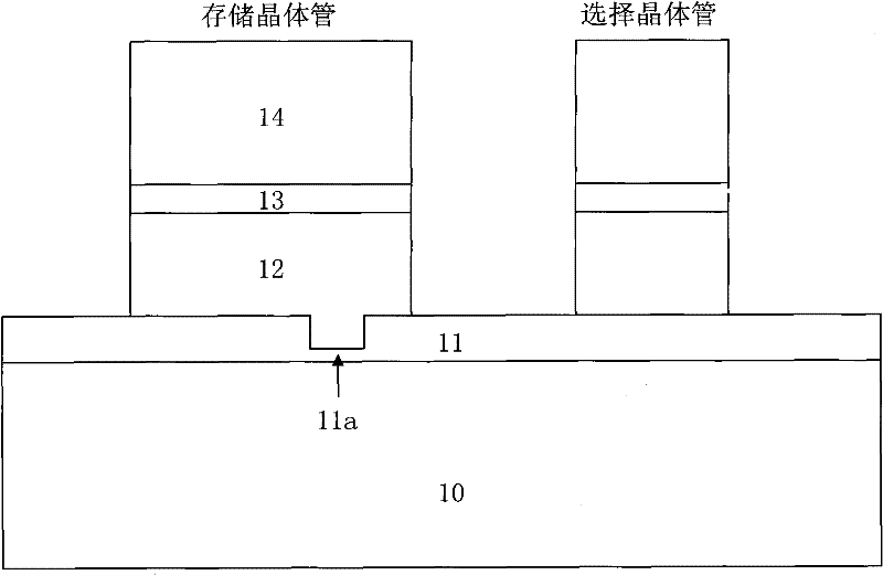
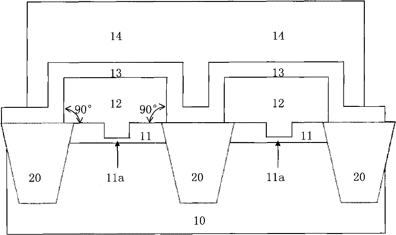
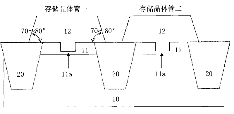
[0019] Step 1, see Figure 3a , which is a schematic cross-sectional view of the EEPROM memory array in the direction of the bit line. Before this step, a gate oxide layer 11 and a tunnel oxide layer 11a have been formed on the silicon substrate 10, an isolation structure 20 has existed in the silicon substrate 10 to isolate each storage transistor, and a silicon substrate 10 has been deposited on the surface. Layer 1500~ thick polysilicon as the floating gate material. The isolation structure 20 is a field oxygen isolation (LOCOS) structure or a shallow trench isolation (STI) structure.

[0020] The operation in this step is to etch the polysilicon layer to form the floating gate 12, the sidewall of the floating gate 12 has an inclination angle of 70-80 degrees. From another perspective, for the trench between the two floating gates 12, it has a tapered etching profile...


PUM


Abstract

The invention discloses a manufacturing method of floating gates of an EEPROM (electrically erasable programmable read-only memory). The method comprises the following steps: 1. etching a polysilicon layer on the surface of a silicon wafer to form floating gates, wherein the side walls of the floating gates have angle of inclination being 70-80 degrees; and the silicon wafer is characterized in that gate oxide layers and tunnelling oxide layers have been formed on the silicon substrate; isolation structures have existed in the silicon substrate; and the polysilicon layer has been deposited onthe surface of the silicon substrate; 2. growing silicon oxide layers on the surfaces of the floating gates by adopting the thermal oxide growth process; and 3. depositing a silicon nitride layer anda silicon oxide layer on the surface of the silicon wafer in sequence, wherein the silicon oxide layers, the silicon nitride layers and the silicon oxide layers on the floating gates form ONO (oxide-nitride-oxide) layers. The topography of the floating gates after etching becomes oblique through improvement and the upper angles of the floating gates are chamfered through the thermal oxide growth process, thus improving the data retention of the EEPROM.

Description

technical field [0001] The invention relates to a manufacturing method of a semiconductor integrated circuit device, in particular to a manufacturing method of an EEPROM. Background technique [0002] see figure 1 , which is a schematic cross-sectional view of the EEPROM array in the word line direction, which shows an EEPROM memory cell, including a storage transistor and a selection transistor. Both transistors are fabricated on substrate 10 and gate oxide 11 . The memory transistor therein also includes a tunnel oxide layer 11 a which is thinner than the gate oxide layer 11 in a small area. The memory transistor also includes a floating gate 12 located below, an ONO (Oxide-Nitride-Oxide) layer 13 located in the middle, and a control gate 14 located above. When the control gate 14 is etched, the ONO layer 13 and the floating gate 12 are etched away together to form isolation between the storage transistor and the selection transistor. [0003] see figure 2 , which is...

Claims


Application Information

Patent Timeline
Patent Type & Authority Applications(China)
IPC IPC(8): H01L21/28H01L21/8247
Inventor 陈广龙陈昊瑜
Owner SHANGHAI HUAHONG GRACE SEMICON MFG CORP
Why Eureka
Try Eureka