
ESD (electrostatic discharge) high-voltage DMOS (diffused metal oxide semiconductor) device and manufacturing method thereof

A high-voltage, device technology, applied in the field of semiconductor integrated circuit manufacturing, can solve the problems of increasing the surface electric field in the drift region, the inability to realize ESD device optimization, and the easy damage of gate oxide, so as to reduce the surface electric field, reduce the trigger voltage, and reduce the conductivity. The effect of on-resistance

Active Publication Date: 2011-07-20
SHANGHAI HUAHONG GRACE SEMICON MFG CORP
View PDF0 Cites 5 Cited by
  • Summary
  • Abstract
  • Description
  • Claims
  • Application Information

AI Technical Summary

Problems solved by technology

However, by increasing the implant dose in the drift region implantation, the optimization of ESD devices cannot usually be achieved. This is because the impurities in the drift region need to go through a high-temperature advancement process. The result of increasing the implant dosage is that the surface and internal concentrations of the drift region increase after the advancement. This will increase the surface electric field in the drift region when triggered, making the gate oxide more susceptible to damage

Method used


Image

  • ESD (electrostatic discharge) high-voltage DMOS (diffused metal oxide semiconductor) device and manufacturing method thereof
  • ESD (electrostatic discharge) high-voltage DMOS (diffused metal oxide semiconductor) device and manufacturing method thereof
  • ESD (electrostatic discharge) high-voltage DMOS (diffused metal oxide semiconductor) device and manufacturing method thereof

Examples


Embodiment Construction

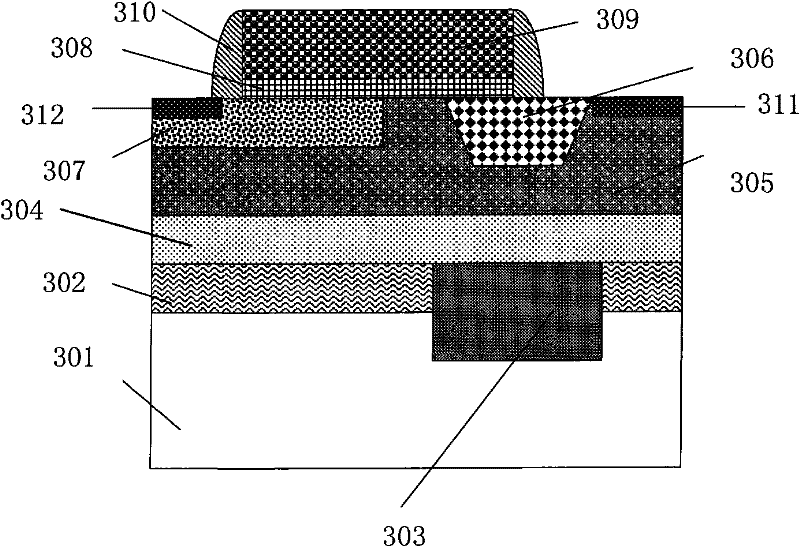
[0025] like figure 1 Shown is the structural representation of the embodiment of the present invention, the embodiment of the present invention is an ESD high voltage N-type DMOS device, comprising:

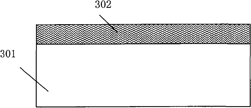
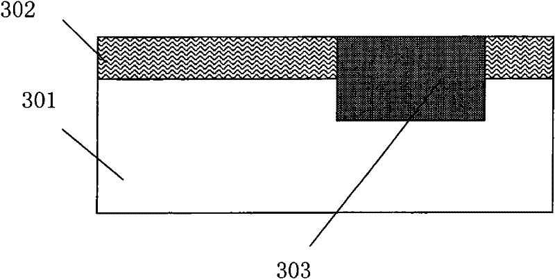
[0026] An N-type lightly doped (N-) drift region 305 is formed by implanting N-type lightly doped ions into the N-silicon epitaxial layer 304, and the silicon epitaxial layer 304 is formed on the N-type heavily doped (N+) buried layer 302 Above, the buried layer 302 is formed on the P-type substrate 301 .

[0027] A P-type channel region 307 is a P-type ion-implanted region formed in the surface part of the drift region 305 .

[0028] An N+ drain region 311 is formed in the surface partial region of the drift region 305 , and a field oxide layer 306 and a surface partial drift region 305 are separated between the drain region 311 and the channel region 307 .

[0029] An N+ source region 312 is formed in the surface part region of the channel region 307 .

[0030] A polysilicon...


PUM


Abstract

The invention discloses an ESD (electrostatic discharge) high-voltage DMOS (diffused metal oxide semiconductor) device which comprises an ESD ion injection region, wherein the ESD ion injection region is formed in part of a drift region under a field oxide layer, impurity ions are injected into a buried layer and enter into the drift region by annealing, propelling and diffusing, and the ESD ion injection region has impurity distribution with gradually reduced concentration between the buried layer and the bottom of the field oxide layer. The invention further discloses a manufacturing methodof the ESD high-voltage DMOS device. By adopting the device and the manufacturing method, the trigger voltage of the device can be effectively reduced, the resistance of the drift region and the on-resistance of the device can be reduced, the strength of a surface electric field of the drift region can be reduced, and a gate oxide can be protected.

Description

technical field [0001] The invention relates to the field of semiconductor integrated circuit manufacturing, in particular to an ESD high-voltage DMOS device, and also relates to a manufacturing method of the ESD high-voltage DMOS device. Background technique [0002] In the BCD process, the design and manufacture of high-voltage ESD devices is an important part of the whole process, and it is also one of the difficulties. The main reasons are: 1. The trigger voltage of ESD high-voltage devices must be accurately designed, which cannot be higher than the breakdown of devices in the internal circuit 2. Carefully design the impurity distribution in the device, optimize the electric field distribution in the device, and try to keep the maximum electric field in the drift region away from the surface when ESD is triggered, so as to avoid damage to the gate oxide when triggered Third, reduce the on-resistance of the ESD device as much as possible, and enhance the device's ability...

Claims


Application Information

Patent Timeline
Patent Type & Authority Applications(China)
IPC IPC(8): H01L29/78H01L29/06H01L29/36H01L23/60H01L21/336H01L21/265
Inventor 钱文生
Owner SHANGHAI HUAHONG GRACE SEMICON MFG CORP
Learn More