Novel silicon substrate heterojunction solar cell

A technology of solar cells and silicon substrates, applied in circuits, photovoltaic power generation, electrical components, etc.

Inactive Publication Date: 2011-08-10
SHANGHAI INST OF SPACE POWER SOURCES
View PDF4 Cites 14 Cited by
  • Summary
  • Abstract
  • Description
  • Claims
  • Application Information

AI Technical Summary

Problems solved by technology

[0005] In order to solve the shortcomings of crystalline silicon solar cells and amorphous silicon solar cells, the technical problem to be solved by the present invention is to propose a new type of solar cell with strong light absorption ability, high efficiency and low cost in combination with the performance characteristics of single crystal silicon and amorphous silicon materials. Silicon based heterojunction solar cells

Method used


Image

  • Novel silicon substrate heterojunction solar cell
  • Novel silicon substrate heterojunction solar cell

Examples


example

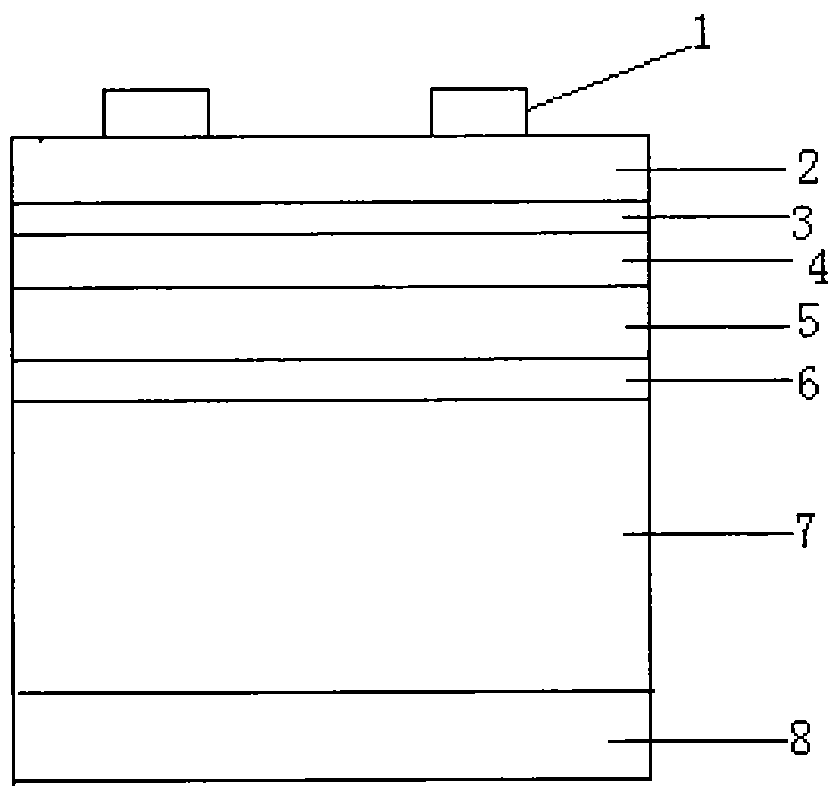
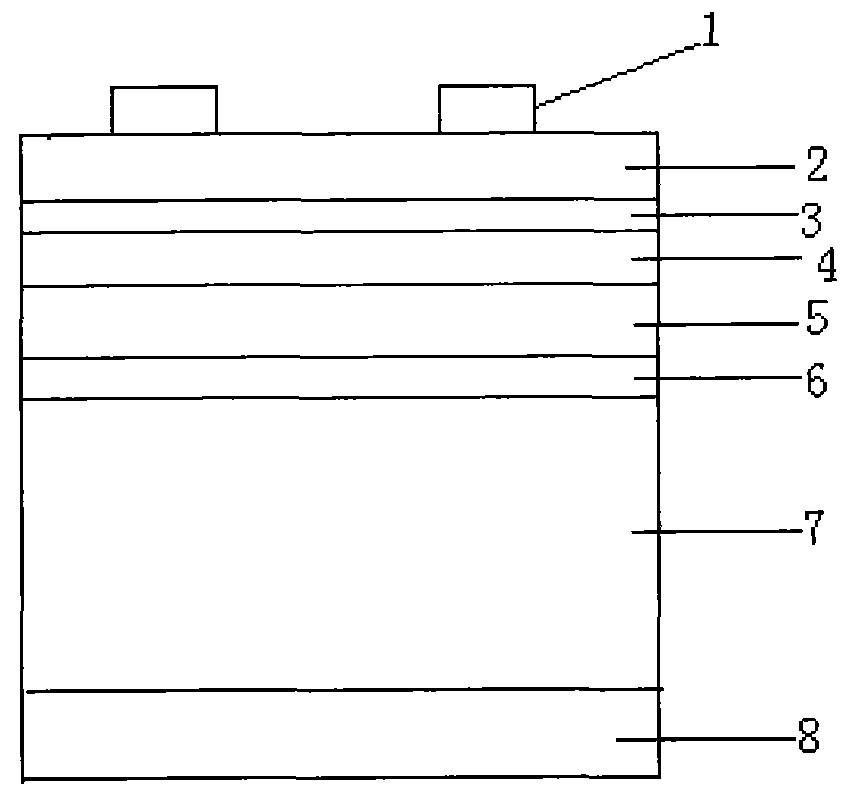
[0027] Such as figure 1 As shown, the silicon substrate 7 is an N-type Czochralski monocrystalline silicon wafer with a crystal orientation of and a resistivity of 2Ω·cm, polished on one side, and a thickness of 260 μm. The thickness of the ITO film 2 grown by magnetron sputtering is 80nm; the thickness of the intrinsic amorphous silicon film 3 deposited by PECVD is 2nm; the thickness of the deposited P-type heavily doped amorphous silicon film 4 is 5nm; the deposited P-type nano-silicon film The thickness of 5 is 12 nm; the thickness of deposited intrinsic amorphous silicon thin film 6 is 3 nm; the thickness of evaporated Ag back electrode 8 is 3 μm.

[0028] After measurement, in the simulated light source AM1.5, 100mW / cm 2 Under the standard light intensity irradiation, the efficiency of the novel silicon-based heterojunction solar cell prepared in this example reaches 17.2%, and the effective area of ​​the cell is 0.28cm 2 , where the open circuit voltage is 602mV and t...


PUM

PropertyMeasurementUnit
thicknessaaaaaaaaaa
thicknessaaaaaaaaaa
thicknessaaaaaaaaaa

Abstract

The invention discloses a novel silicon substrate heterojunction solar cell. An Ag back electrode is formed on the back surface of an N-type monocrystalline silicon or polycrystalline silicon slice through evaporation; intrinsic amorphous silicon (i-a-Si:H), P-type nanosilicon (p-nc-Si:H), P-type heavily doped amorphous silicon (p+-a-Si:H) and ultrathin intrinsic amorphous silicon (i-a-Si:H) are deposited on the front surface (light receiving surface of a cell) of the silicon slice in sequence; finally an ITO (Indium Tin Oxide) transparent conductive thin film is sputtered on the silicon; and an Ag gate line electrode is printed by a screen. The solar cell with the novel structure has lower cost than that of the normal silicon solar cell, so that the light-induced degradation of the normal amorphous silicon solar cell is reduced, and the cell has higher stability in long-term use, high light absorbing capacity and high photoelectric conversion efficiency. The efficiency reaches 17.2 percent at the standard analog light intensity of AM1.5, 100mW / cm<2>.

Description

technical field [0001] The invention relates to the technical field of semiconductor solar cells, in particular to a silicon-based heterojunction solar cell structure. Background technique [0002] At present, in the international market, crystalline silicon and polycrystalline silicon solar cells occupy a leading position in the market due to their high conversion efficiency and mature production technology. However, the high temperature (above 900°C) diffusion junction process used in the production of these traditional silicon solar cells consumes a lot of energy, so the production cost is high. With the development of photovoltaic industry technology, it is necessary to adopt new technologies and methods to prepare solar cells to reduce Production costs and further improvement of conversion efficiency, thereby opening up a wider market. [0003] The production of thin-film solar cells by low-temperature thin-film preparation technology is a new direction of solar cell r...

Claims


Application Information

Patent Timeline
Patent Type & Authority Applications(China)
IPC IPC(8): H01L31/075H01L31/028H01L31/20
CPCY02E10/50Y02E10/547Y02E10/548Y02P70/50
Inventor 柳琴叶晓军刘成周丽华钱子勍张翼翔
Owner SHANGHAI INST OF SPACE POWER SOURCES
Why Eureka
Try Eureka