Boron gettering method for metallurgical N-type polycrystalline silicon chip

A polycrystalline silicon wafer, metallurgical technology, applied in chemical instruments and methods, silicon compounds, non-metallic elements, etc., can solve the problems of high diffusion temperature, long diffusion time, small phosphorus diffusion coefficient, etc., to achieve high doping concentration, diffusion Uniform and repeatable results

Inactive Publication Date: 2011-08-17
XIAMEN UNIV
View PDF2 Cites 10 Cited by
  • Summary
  • Abstract
  • Description
  • Claims
  • Application Information

AI Technical Summary

Problems solved by technology

However, the diffusion coefficient of phosphorus in silicon is very small, and a higher diffusion temperature and a longer diffusion time are required to achieve the gettering effect.

Method used


Image

  • Boron gettering method for metallurgical N-type polycrystalline silicon chip
  • Boron gettering method for metallurgical N-type polycrystalline silicon chip
  • Boron gettering method for metallurgical N-type polycrystalline silicon chip

Examples


Embodiment 1

[0031] (1) Clean metallurgical N-type polycrystalline silicon wafers with RCA liquid and dry them; RCA liquid cleaning includes: No. III liquid H 2 SO 4 : H 2 O 2 =4:1; No. I liquid NH 4 OH:H 2 O 2 : H 2 O=1:2:5; No. II solution HCl:H 2 O 2 : H 2 O=1:2:8. H 2 SO 4 , H 2 O 2 , NH 4 Both OH and HCl are excellent grade pure, with mass fractions of 95-98%, 30%, 25-28%, and 36-38%, respectively. The three solutions are formulated in volume ratio.

[0032] (2) Passing the silicon wafer obtained in step (1) into trimethyl borate B (CH) at a temperature of 900° C. 3 O) 3Carry out 1.5h boron gettering treatment, the gas flow used is large N 2 1L / min, small N 2 0.02L / min, the silicon wafer is naturally cooled in the air.

[0033] (3) soak the silicon wafer obtained in step (2) in dilute HF (HF:H 2 O=1:10) solution for 10min, then use HF:HNO 3 (1:3) Soak in acid etching solution for 30s, wash with deionized water for several times, and dry. The mass percentage conce...

Embodiment 2

[0036] Same as embodiment 1, its difference is that the temperature and time of boron gettering heat treatment are different, and step (2) is:

[0037] (2) Pass the silicon wafer obtained in step (1) into B(CH) in a four-tube microcomputer diffusion furnace at a temperature of 920°C 3 O) 3 Carry out 2h boron gettering treatment, the gas flow used is large N 2 1L / min, small N 2 0.02L / min, the silicon wafer is naturally cooled in the air.

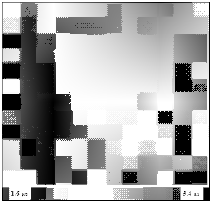
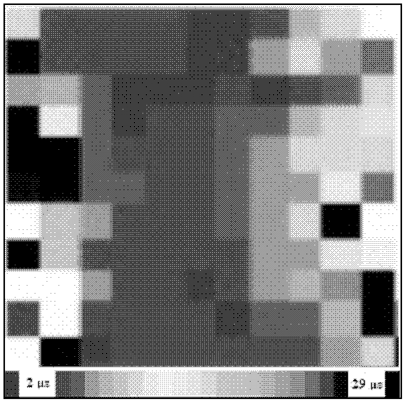
[0038] Test the resistivity of the silicon wafer obtained in step (3); test the minority carrier lifetime of the silicon wafer after depositing 80 nm of silicon nitride on both sides by PECVD. The test method is the same as that of Example 1. Minority carrier lifetime distribution figure 2 As shown, the resistivity increased from 0.20 Ω·cm to 0.56 Ω·cm.

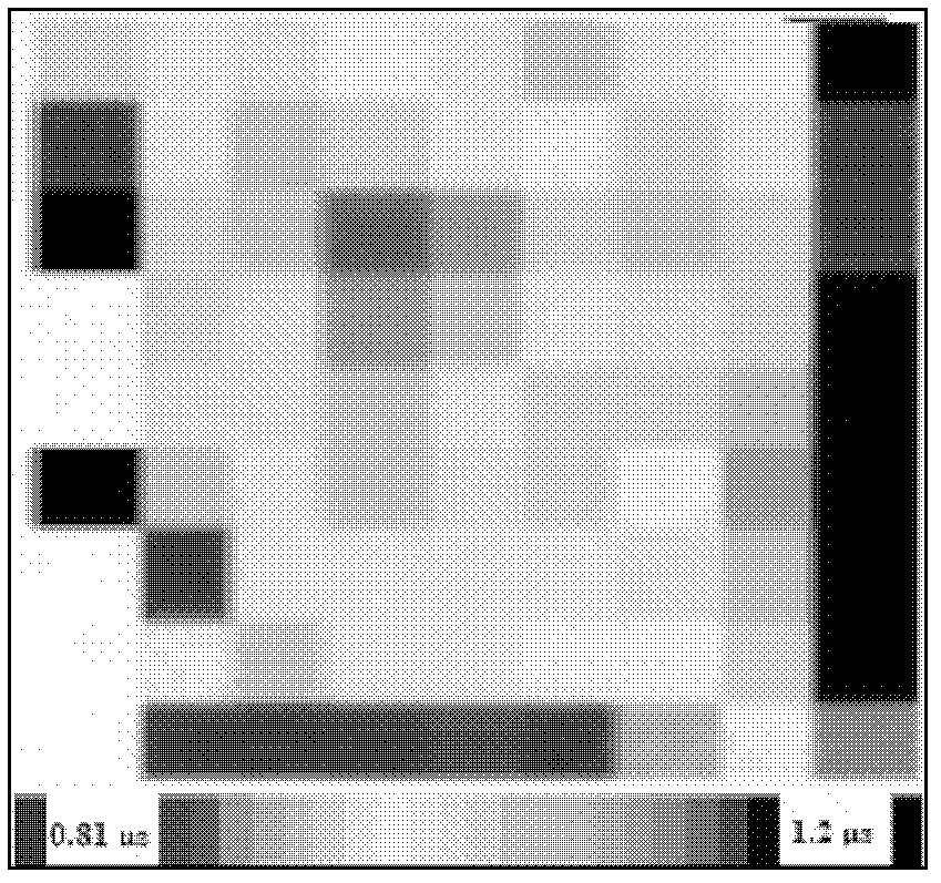
[0039] Minority carrier lifetime distribution of the original silicon wafer without gettering treatment (average 1.2μs) see image 3 .


PUM

PropertyMeasurementUnit
electrical resistivityaaaaaaaaaa
thicknessaaaaaaaaaa
depthaaaaaaaaaa

Abstract

The invention discloses a boron gettering method for a metallurgical N-type polycrystalline silicon chip, and relates to polycrystalline silicon. The invention provides the boron gettering method for the metallurgical N-type polycrystalline silicon chip, which has good gettering effect, low cost and simple operation and is suitable for industrialized production. The method comprises the followingsteps of: cleaning and drying the metallurgical N-type polycrystalline silicon chip; introducing gas to the obtained silicon chip at the temperature of between 700 and 1,200 DEG C to perform boron diffusion gettering heat treatment, and then cooling the silicon chip; soaking the obtained silicon chip into hydrofluoric acid (HF) solution; and corroding the gettering layer on the obtained silicon chip by using acid corrosive liquid, and cleaning, drying and baking the obtained silicon chip to obtain a boron gettered polycrystalline silicon chip.

Description

technical field [0001] The invention relates to polysilicon, in particular to a boron gettering method for metallurgical N-type polycrystalline silicon wafers. Background technique [0002] High efficiency and low cost are the main trends in the development of solar cells. The low price and high conversion efficiency of polycrystalline silicon solar cells have become a research hotspot in the international photovoltaic industry. At present, the production of solar-grade polysilicon generally adopts the modified Siemens method, but the cost is high, and the technology is monopolized by foreign countries, which leads to the shortage of this material and the high price. Currently, more and more researchers and manufacturers are focusing on metallurgically purified polysilicon. The technology of metallurgical purification of silicon (Wu Hongjun, Chen Xiuhua, Ma Wenhui, et al. Research status of polysilicon for solar cells and its gettering [J]. Materials Review, 2010, 15: 135-...

Claims


Application Information

Patent Timeline
Patent Type & Authority Applications(China)
IPC IPC(8): C01B33/037
Inventor 陈朝郑兰花潘淼李艳华杨倩徐进
Owner XIAMEN UNIV
Why Eureka
Try Eureka