Rubrene weak epitaxial growth thin film and application thereof in organic thin-film transistor

A weak epitaxial growth, rubrene technology, applied in the direction of crystal growth, single crystal growth, single crystal growth, etc., can solve the problems of complex process, poor quality of polycrystalline film, etc., to achieve the effect of simple process

Inactive Publication Date: 2013-12-04
CHANGCHUN SHENGZHUOLONG ELECTRONICS MATERIALS
View PDF1 Cites 0 Cited by
  • Summary
  • Abstract
  • Description
  • Claims
  • Application Information

AI Technical Summary

Problems solved by technology

[0004] In order to overcome the problems of complex process and poor quality of polycrystalline film in the preparation process of existing rubrene polycrystalline film, the present invention provides a rubrene weak epitaxial growth film

Method used


Image

  • Rubrene weak epitaxial growth thin film and application thereof in organic thin-film transistor
  • Rubrene weak epitaxial growth thin film and application thereof in organic thin-film transistor
  • Rubrene weak epitaxial growth thin film and application thereof in organic thin-film transistor

Examples


Embodiment 1

[0074] The preparation method of rubrene weak epitaxial growth film involved in the present invention is as follows

[0075] (1) A layer of SiO is formed by thermal growth on the surface 2 The heavily doped silicon wafer surface vacuum deposition induction layer 3; The material of the induction layer 3 is: hexabiphenyl (p-6P), 2,7-two (4-biphenyl)-phenanthrene (BPPh), 2,7-bis(4-biphenyl)-thiofluorene (BPBTB), 2,6-bis(4-biphenyl)-benzo[1,2-b:4,5-b']dithiophene (BPTBT), 2,5-bis(4-biphenyl)-[3,2-b]dithiophene (BPTT), 5,5'-bis(4-biphenyl)-2,2'- Dithiophene (BP2T), 5,5″-bis(4-biphenyl)-2,2′:5′,2″-trithiophene (BP3T), 5,5″′-bis(4-biphenyl) )-2, 2': 5', 2": 5", 2"'-tetrathiophene (BP4T), 1, 1': 4', 1": 4", 1"': 4"', 1" ″: 4″″, 1″″′: 4″″′, 1″″″: 4″″″, 1″″″′-octyl (p8P), 2,5-di(4-1,1 ': 4', 1"-terphenyl)-thiophene (3PT), 5,5'-di(4-1,1': 4', 1"-terphenyl)-2,2'-dithiophene (3P2T), 2,5-bis(4-1,1′:4′,1″-terphenyl)-[3,2-b]dithiophene (3PTT), 2,7-bis(4- 4′-fluorobiphenyl)-phenanthrene ...

Embodiment 2

[0089] The first kind of structure that the present invention relates to adopts the transistor of rubrene weak epitaxial growth film, such as Figure 6 As shown, the preparation method is as follows:

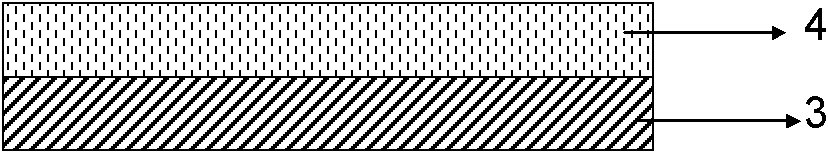
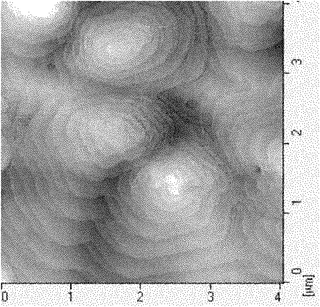
[0090] (1) A layer of SiO is formed by thermal growth on the surface 2 The heavily doped silicon wafer surface vacuum-deposits induction layer 3, and the material of described induction layer 3 is the same as embodiment 1, and thickness is not less than 2 nanometers, is not more than 12 nanometers; Described heavily doped silicon is used as transistor gate electrode, SiO 2 as the insulated gate of the transistor;

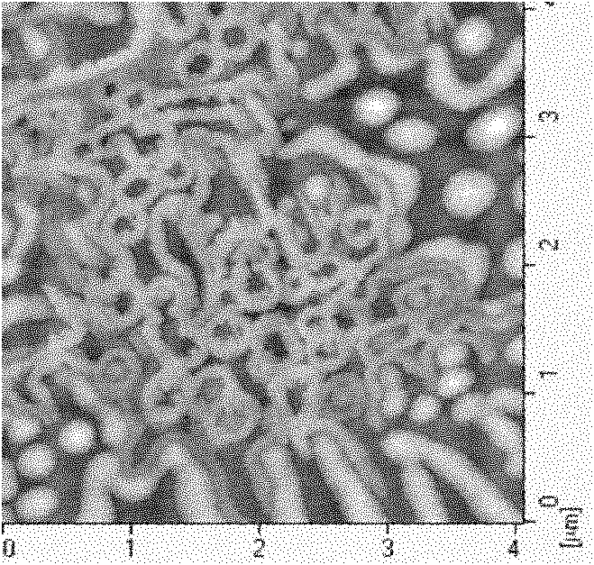
[0091] (2) Vacuum-deposit rubrene film 4 on the surface of induction layer 3, the thickness of said rubrene film 4 is not less than 5 nanometers, not more than 50 nanometers;

[0092] (3) On the surface of the rubrene film 4, a metal gold electrode 6 is vacuum-deposited by a leak mask method;

[0093] Among them, the background vacuum degree is not lower than 1×10 ...

Embodiment 3

[0100] The device configuration of the transistor with the second structure that uses rubrene weakly epitaxially grown thin film is as follows Figure 8 As shown, the specific preparation method is as follows:

[0101] (1) A layer of SiO is formed by thermal growth on the surface 2 The heavily doped silicon wafer surface vacuum-deposits induction layer 3, and the material of described induction layer 3 is the same as embodiment 1, and thickness is not less than 2 nanometers, is not more than 12 nanometers; Described heavily doped silicon is used as transistor gate electrode, SiO 2 as the insulated gate of the transistor;

[0102] (2) On the surface of the induction layer 3, a metal gold electrode 6 is vacuum-deposited by a leak mask method;

[0103] (3) Vacuum-deposit a rubrene film 4 on the surface of the induction layer 3, the thickness of the rubrene film 4 is not less than 5 nanometers, not more than 50 nanometers;

[0104] Among them, the background vacuum degree is no...


PUM

PropertyMeasurementUnit
thicknessaaaaaaaaaa
thicknessaaaaaaaaaa
thicknessaaaaaaaaaa

Abstract

The invention provides a rubrene weak epitaxial growth thin film and an application thereof in an organic thin-film transistor. By utilizing an epitaxial relation between the crystal of an induction layer material and the lattice of a rubrene crystal, rubrene molecules are subjected to epitaxial growth on the surface of a large-area continuous orderly induction layer so as to acquire a high-quality polycrystal thin film. In the invention, the rubrene polycrystal thin film is prepared by utilizing a weak epitaxial growth method and a conventional vacuum deposition technology, the process is simple, and the rubrene thin film prepared through the weak epitaxial growth has the characteristics of larger crystal size and good continuity. With respect to the transmittance spectrum of a 30nm of the rubrene weak epiaxial growth thin film, the light transmittance of the rubrene is larger than 90% in a visible light area and the rubrene weak epiaxial growth thin film can be used as a transparent material. The mobility of a prepared thin-film transistor is up to 1.4-3.6cm<2> / Vs, exceeds the mobility of an amorphous silicon thin-film transistor by 0.7cm<2> / Vs and is 2-5.2 times higher than that of the amorphous silicon.

Description

technical field [0001] The invention relates to a weak epitaxial growth film of rubrene and the application of this film in organic thin film transistors. technical background [0002] 5, 6, 11, 12-tetraphenyltetracene (commonly known as rubrene), as a high-mobility organic semiconductor material, has recently attracted widespread attention. Its single crystal mobility can reach 15-40cm 2 / Vs(J. Takeya, M. Yamagishi, Y. Tominari, R. Hirahara, Y. Nakazawa, T. Nishikawa, T. Kawase, T. Shimoda, S. Ogawa, Appl. Phys. Lett. 2007, 90, 102120 ), which is the highest value reported so far for organic semiconductors. In addition, rubrene has a large band gap and low light absorption coefficient, and its thin film can be approximated as a transparent material in the visible range, so it has potential application prospects in display driving. However, the thin film of this material prepared by traditional vacuum deposition is usually amorphous, and the performance of the thin film t...

Claims


Application Information

Patent Timeline
Patent Type & Authority Patents(China)
IPC IPC(8): C30B23/02C30B29/54H01L51/05H01L51/30
Inventor 王彤黄丽珍
Owner CHANGCHUN SHENGZHUOLONG ELECTRONICS MATERIALS
Why Eureka
Try Eureka