Melting sealing cap-sealing process-based chip vacuum eutectic welding method

A vacuum eutectic welding and chip technology, which is applied in the field of chip vacuum eutectic welding and chip vacuum eutectic welding based on the melting capping process, can solve problems such as low welding temperature, achieve welding void control, and reduce the formation of voids. chance, the effect of increasing the level of consistency

Inactive Publication Date: 2011-08-17
BEIJING MXTRONICS CORP +1
View PDF5 Cites 17 Cited by
  • Summary
  • Abstract
  • Description
  • Claims
  • Application Information

AI Technical Summary

Problems solved by technology

This process needs to have excellent electrical and thermal conductivity, and the chip loading process requires a relatively low soldering temperature to avoid the impact of high temperature on the internal structure of the chip; at the same time, it is also necessary to ensure that the chip soldering material is not produced when the cap is welded. secondary melting, and the existing eutectic solder welding using parallel seam welding process cannot meet the above needs, so it is urgent to study a new eutectic solder welding method

Method used


Image

  • Melting sealing cap-sealing process-based chip vacuum eutectic welding method
  • Melting sealing cap-sealing process-based chip vacuum eutectic welding method
  • Melting sealing cap-sealing process-based chip vacuum eutectic welding method

Examples


Embodiment Construction

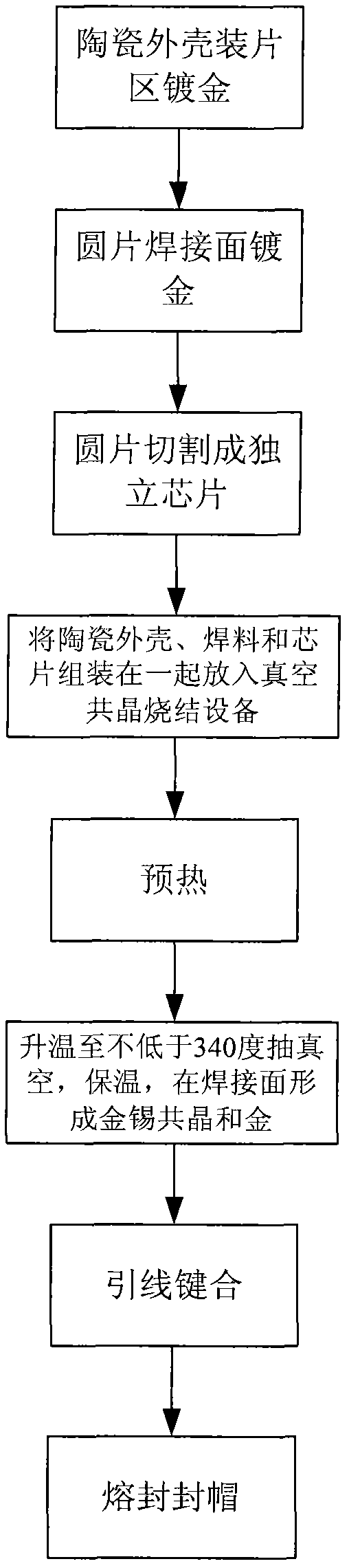
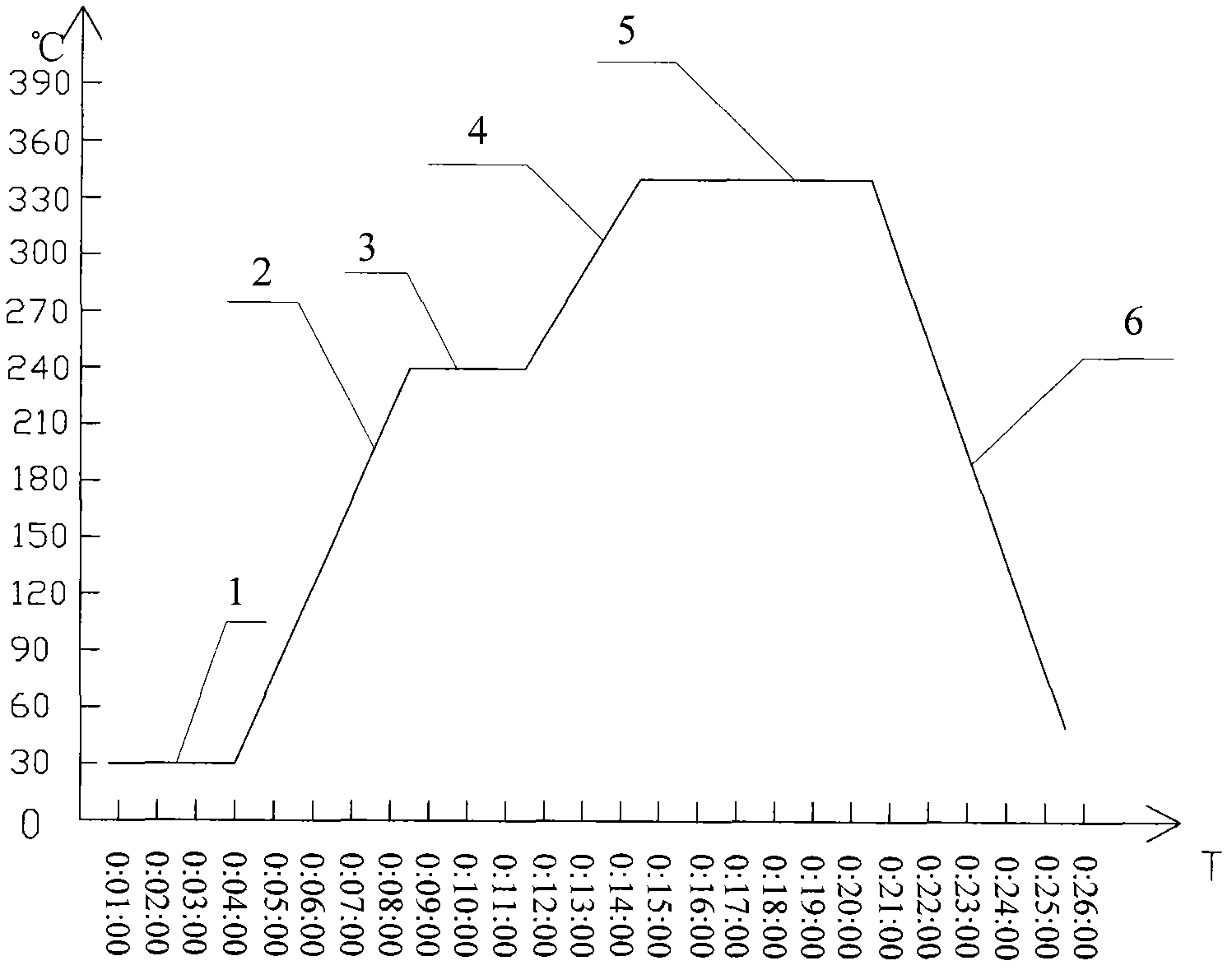
[0030] The present invention as figure 1 shown in the following steps:

[0031] 1. A layer of gold plating is formed on the chip loading area of ​​the ceramic shell, and the thickness of the gold plating is 1.3-2 μm.

[0032] 2. Form a layer of Ti-Ni-Au coating on the welding surface of the wafer, and the thickness of the Ti layer in the Ti-Ni-Au coating is Ni layer thickness is The thickness of the Au layer is

[0033] 3. Scribing the wafer formed with the Ti-Ni-Au coating into individual chips.

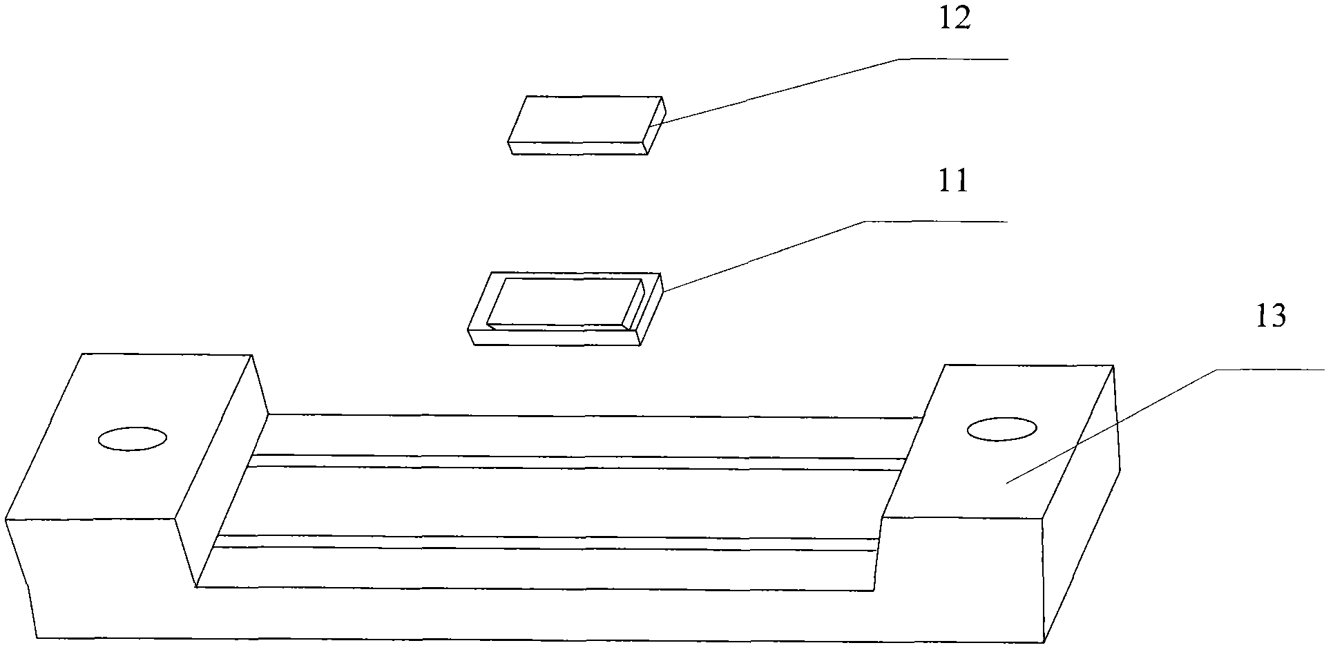
[0034] 4. Use a special fixture to assemble the ceramic shell, solder and chips together and put them into the vacuum eutectic sintering equipment.

[0035] Special fixtures such as figure 2 As shown, it includes a positioning block 1, a pressing block 2 and a base 3. The base 3 is processed with a groove for installing a ceramic shell. The ceramic shell is installed in the groove of the base 3. The positioning block 1 is installed on the ceramic shell. Solder and chip ar...


PUM

PropertyMeasurementUnit
thicknessaaaaaaaaaa

Abstract

The invention discloses a melting sealing cap-sealing process-based chip vacuum eutectic welding method. The technical difficult problems that the conventional vacuum eutectic welding cannot adopt a melting sealing cap-sealing process are solved by performing gold-plating, slicing, vacuum eutectic welding, lead wire bonding, gold-stannum alloy melting-sealing cap-sealing and the like on a ceramic shell and a wafer. In the method, the welding temperature is 340 DEG C and the heat insulation time is 6 minutes; the time and the temperature are both higher than those of conventional welding conditions so that a welding flux is permeated into the chip loading surface of the ceramic shell and the chip surface to change the components of Au / Sn in the welding flux; therefore, the problem of secondary melting in a chip welding area when performing the melting-sealing cap-sealing is avoided. In the method, vacuumizing is performed after melting the welding flux, most of air bubbles formed when welding the chip are vacuumized so as to effectively reduce the cavity formation probability of the welding area; therefore, welding cavities are controlled effectively. The chip bonding method adopted by the invention is on the basis of the melting-sealing cap-sealing process, contributes to batch production of the overall packaging production and improves the consistency level of products.

Description

technical field [0001] The invention relates to a vacuum eutectic welding method for a chip, in particular to a vacuum eutectic welding method for a chip based on a fusion-sealing and capping process, and belongs to the technical field of integrated circuit packaging. Background technique [0002] Conventional die attach methods include: epoxy bonding, friction eutectic and eutectic solder bonding. Conventional capping processes include parallel seam welding process and fusion sealing process. If the chip mounting method of epoxy resin bonding is adopted, the cap sealing process may adopt a parallel seam welding process or a fusion sealing process. Since gold-tin alloy has the characteristics of high thermal conductivity and low soldering temperature, eutectic solder soldering using gold-tin alloy solder is the best choice for ceramic shell chip soldering. However, for circuits that are conventionally mounted using gold-tin solder welding process, since gold-tin alloy is a...

Claims


Application Information

Patent Timeline
Patent Type & Authority Applications(China)
IPC IPC(8): H01L21/60
CPCH01L2924/0002
Inventor 冯小成陈建安练滨浩姚全斌
Owner BEIJING MXTRONICS CORP
Why Eureka
Try Eureka