GaN-based light emitting diode and preparation method thereof

A technology of light-emitting diodes and emission layers, which is applied in the direction of electrical components, circuits, semiconductor devices, etc., can solve the problems of sensitive luminous performance, difficult control of triangular quantum wells, and the stability and repeatability of LED devices need to be improved, so as to improve the luminescence Efficiency, improvement of light output reliability and repeatability, effects of mitigating polarization effects

Inactive Publication Date: 2011-08-17
SUN YAT SEN UNIV
View PDF5 Cites 49 Cited by
  • Summary
  • Abstract
  • Description
  • Claims
  • Application Information

AI Technical Summary

Problems solved by technology

However, due to the current MOCVD and other deposition technologies and the performance limitations of related instruments and equipment, it is very difficult to control the triangular quantum well with gradual

Method used


Image

  • GaN-based light emitting diode and preparation method thereof
  • GaN-based light emitting diode and preparation method thereof
  • GaN-based light emitting diode and preparation method thereof

Examples


Embodiment 1

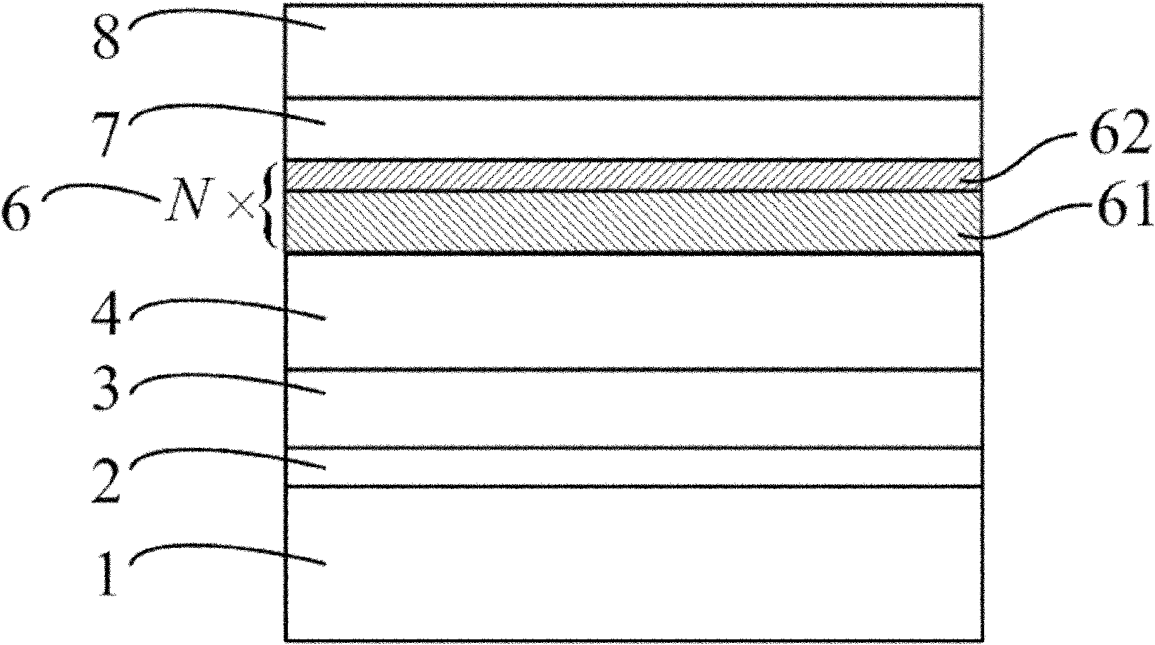
[0047] 1. Using ordinary metal oxide vapor deposition (MOCVD) equipment, the substrate material 1 is a sapphire non-patterned (0001) surface substrate; heat at high temperature to clean the substrate; then lower the temperature to grow the GaN initial growth layer 2. The thickness is 20nm;

[0048] 2. On the basis of step 1, raise the temperature, recrystallize the GaN layer, and then grow sequentially:

[0049] GaN buffer layer 3, which is a non-doped GaN layer with a thickness of 1 μm;

[0050] n-type electron injection layer 4, which is a Si-doped GaN layer with a thickness of 2.3 μm;

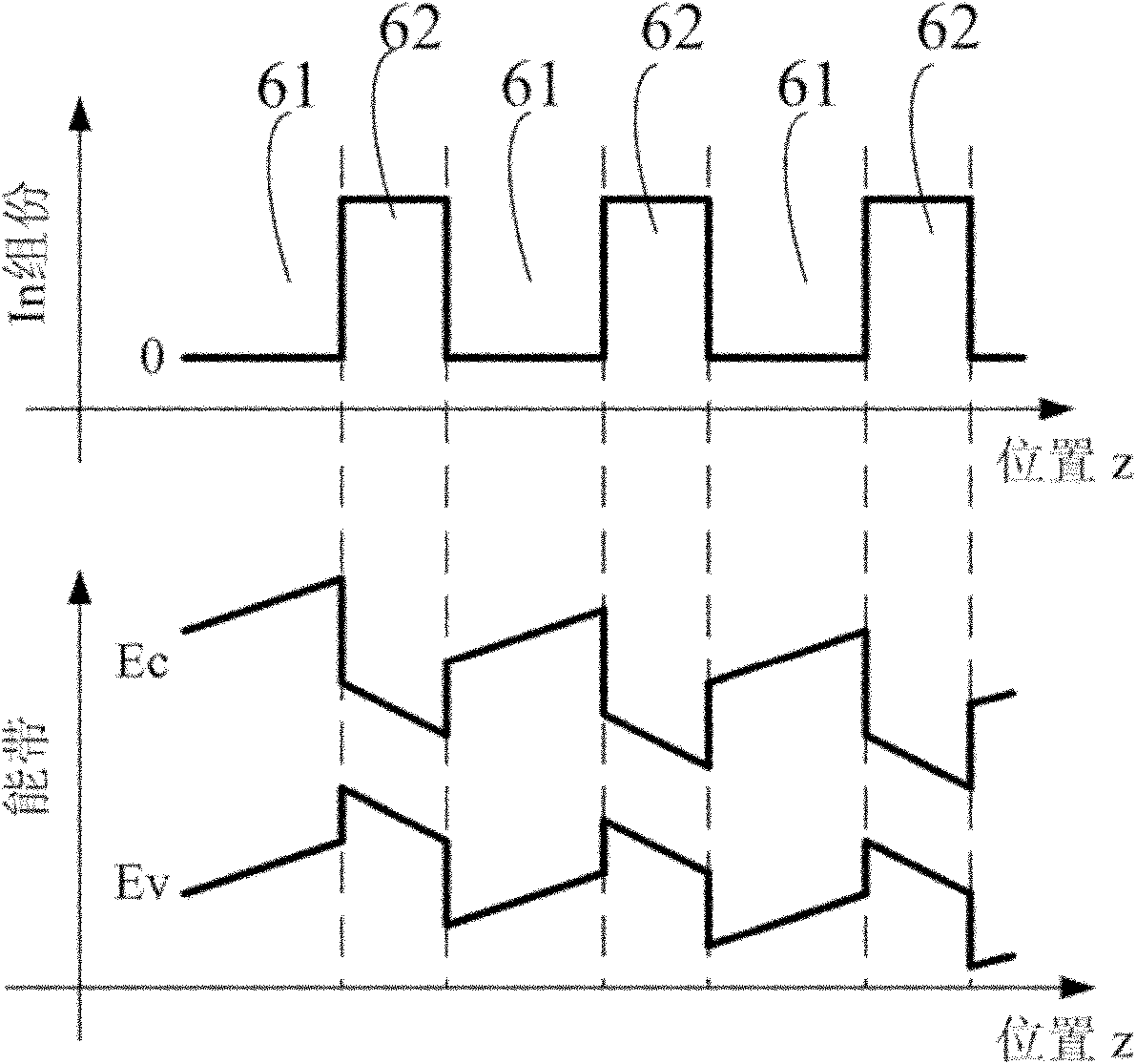
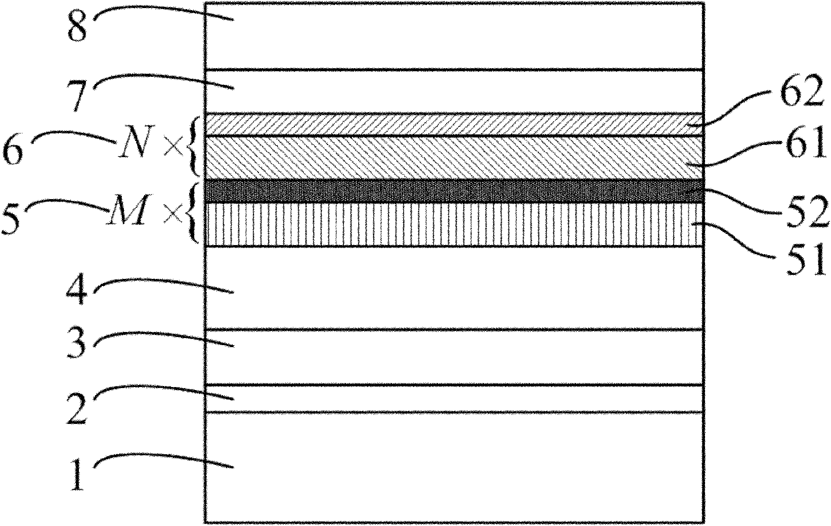
[0051] 3. On the basis of step 2, the temperature is reduced to grow the shallow quantum well structure electron emission layer 5, and a total of 3 periods of barrier layers 51 and shallow quantum well layers 52 are grown; wherein:

[0052] The barrier layer 51 is a Si-doped GaN material with a thickness of 7nm;

[0053] The shallow quantum well layer 52 is InGaN with a triangular structu...

Embodiment 2

[0060] 1. Using ordinary metal oxide vapor deposition (MOCVD) equipment, the substrate material 1 is a non-patterned silicon (0001) surface substrate; heat at high temperature to clean the substrate; then lower the temperature to grow AlN initial growth Layer 2 with a thickness of 50nm;

[0061] 2. On the basis of step 1, heat up and grow sequentially:

[0062] GaN buffer layer 3, which is a non-doped GaN layer with a thickness of 1 μm;

[0063] n-type electron injection layer 4, which is a Si-doped GaN layer with a thickness of 2.3 μm;

[0064] 3. On the basis of step 2, reduce the temperature to grow the shallow quantum well structure electron emission layer 5, and grow a total of 3 cycles, the barrier layer 51 and the shallow quantum well layer 52; wherein:

[0065] The barrier layer 51 is a Si-doped AlInGaN material with a thickness of 7nm;

[0066] The shallow quantum well layer 52 is InGaN with a triangular structure, that is, the non-doped InGaN whose In composition ...

Embodiment 3

[0074] 1. Using ordinary metal oxide vapor deposition (MOCVD) equipment, the substrate material 1 is a patterned sapphire substrate, the pattern is a hemispherical pattern arranged regularly, and the growth surface is a (0001) surface; clean the substrate at high temperature; then put Lowering the temperature to grow GaN initial growth layer 2 with a thickness of 20nm;

[0075] 2. On the basis of step 1, increase the temperature to recrystallize the GaN layer, and then grow sequentially:

[0076] GaN buffer layer 3, which is a non-doped GaN layer with a thickness of 3 μm;

[0077] n-type electron injection layer 4, which is a Si-doped GaN layer with a thickness of 2 μm;

[0078] 3. On the basis of step 2, reduce the temperature to grow the shallow quantum well structure electron emission layer 5, and grow a total of 3 cycles, the barrier layer 51 and the shallow quantum well layer 52;

[0079] Wherein: the barrier layer 51 is a Si-doped GaN material with a thickness of 7nm; ...


PUM

PropertyMeasurementUnit
Thicknessaaaaaaaaaa
Thicknessaaaaaaaaaa
Thicknessaaaaaaaaaa

Abstract

The invention relates to a GaN-based light emitting diode and a preparation method thereof. An initial growth layer, a GaN buffer layer, an n-type electronic injection layer, a quantum well structure electronic emission layer, a quantum well structure light emitting active layer, a p-type AlInGaN electronic stopping layer and a p-type cavity injection layer are grown on an epitaxial substrate of the light emitting diode sequentially; in the quantum well structure of the electronic emission layer, the width of a forbidden band of the AlInGaN quantum well layer in the emission layer is greater than that of the forbidden band of the AlInGaN quantum well in the light emitting active layer; and the AlInGaN quantum well layer of the quantum well structure electronic emission layer is triangular. The GaN-based light emitting diode has the advantages that the quantum well structure electronic emission layer can improve the efficiency of an electronic injection light emitting active layer effectively; and by the triangular quantum well structure of the electronic emission layer, the polarization effect of the epitaxial substrate of the light emitting diode can be reduced, and the working voltage of the light emitting diode is decreased.

Description

technical field [0001] The invention belongs to the field of light-emitting diodes, and in particular relates to a GaN-based light-emitting diode. The invention also includes a manufacturing method of the light-emitting diode. Background technique [0002] A light-emitting diode (Light-emitting diode, LED) is an injection electroluminescent device. Due to the advantages of LED in energy saving and intelligent control, it has received widespread attention. In particular, LEDs based on GaN-based materials (AlN, InN, GaN and their compounds) have become the mainstream direction of LED development because of their adjustable wavelength range theoretically covering the entire visible and ultraviolet bands. Since the beginning of the 21st century, LED technology represented by GaN-based blue LEDs has made great progress in both research and commercial production applications, and its application fields have become more and more open. However, at present, the luminous efficiency ...

Claims


Application Information

Patent Timeline
IPC IPC(8): H01L33/32H01L33/04H01L33/00
Inventor 江灏王钢黄善津
Owner SUN YAT SEN UNIV
Why Eureka
Try Eureka