Organic resistive random access memory (RRAM) with peak shaped bottom electrode and manufacture method thereof

A resistive memory, bottom electrode technology, applied in the field of microelectronics, can solve problems such as unfavorable device repeatability and stability, and achieve the effect of enhancing repeatability

Inactive Publication Date: 2011-08-17
FUDAN UNIV
View PDF2 Cites 7 Cited by
  • Summary
  • Abstract
  • Description
  • Claims
  • Application Information

AI Technical Summary

Problems solved by technology

Obviously, for such a structure, the electric field distribution in the dielectric layer is generally uniform, so the position where the filament appears at the electrode has a certain randomness, which is not conducive to the repeatability and stability of the device.

Method used


Image

  • Organic resistive random access memory (RRAM) with peak shaped bottom electrode and manufacture method thereof
  • Organic resistive random access memory (RRAM) with peak shaped bottom electrode and manufacture method thereof
  • Organic resistive random access memory (RRAM) with peak shaped bottom electrode and manufacture method thereof

Examples


Embodiment Construction

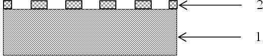
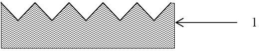
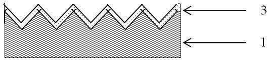
[0031] The present invention is further described below through specific process steps, wherein the top electrode and the bottom electrode are selected from metal Al material as an example, and the organic medium layer is selected from PEDOT:PSS as an example:

[0032] 1. Use conventional integrated circuit technology to obtain a standard P-type device-level substrate Si (100) sheet without graphics, with a resistivity of 6-10 Ω cm. After standard RCA cleaning process, use a 2% HF dilution solution to remove silicon Intrinsic oxide layer on the chip surface.

[0033] 2. Spin-coat the positive resist on a large area and perform photolithography. After developing, a dot-shaped pattern is formed, and the diameter of the dot is 50nm. Use the RIE method to use oxygen plasma to treat the sample as a base film to remove the positive glue in the non-masked area. The oxygen flow rate is 20sccm, the power is 75W, the time is 45s, and the air pressure is 4Pa, such as figure 1 shown.

...


PUM

PropertyMeasurementUnit
Diameteraaaaaaaaaa
Diameteraaaaaaaaaa

Abstract

The invention belongs to the technical field of microelectronics, specifically relates to an organic resistive random access memory (RRAM) with peak shaped bottom electrode and flat top electrode and a manufacture method thereof. The method related by the invention comprises steps of: first manufacturing a substrate with peak figures; and depositing a bottom electrode, spin coating an organic medium layer and depositing a top electrode in turn; finally forming an organic RRAM device with a peak shaped bottom electrode. The RRAM with the peak shaped bottom electrode can form a certain electric field distribution on the medium layer, and the electric field at the peak part is maximum, so conductive filaments are formed preferentially at the peak part, thereby improving the repeatability and current switch rate of the RRAM well. The method of invention is suitable for the organic RRAM device based on filament conduction principle.

Description

Technical field [0001] The invention is a microelectronics technology field, which involves an organic blocking memory and its preparation methods. Background technique [0002] The characteristics of data preservation can be divided into two categories: data preservation.Among them, susceptible devices mainly include SRAM and DRAM, which have been widely researched and put into industrial production.In the non -erratic device, the Flash device occupies the vast majority of market share due to its high density and low cost characteristics.However, the Flash device is suffering from low durability, low -writing speed, and high -writing voltage. On the other hand, it is difficult to reduce the ratio of the Flash device further.In this case, several other non -easy -to -loss memory, including Fram, MRAM, PRAM, and RRAM, have received widespread attention and research.Among them, RRAM, based on the characteristics of electrical resistance, (organic blocking memory), is particularly n...

Claims


Application Information

Patent Timeline
IPC IPC(8): H01L51/00
Inventor 于浩王井舟蒋玉龙茹国平屈新萍李炳宗
Owner FUDAN UNIV
Why Eureka
Try Eureka